Nov 14 2017
Scientists from KAUST have ascertained the electronic properties of an interface between two wide bandgap semiconductors. This understanding will assist in enhancing the efficiency of high-power and light-emitting electronic devices.
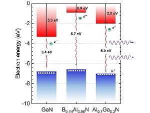 Knowledge of the bandgap and band alignment of aluminum-nitride-based semiconductors is key to designing energy-efficient optical and power devices. CREDIT: 2017 KAUST.
The electrical characteristics of semiconductors (e.g. gallium nitride and silicon) stand in between those of an insulator and a conductor. They permit the flow of current only if electrons gain adequate energy to cross a barrier called the bandgap, which may be indirect or direct, narrow or large, and governs the characteristics of semiconductors and their resultant uses.
For instance, materials that have a large bandgap are applicable in high-power electronics as they have higher breakdown voltage for energy-effective transistors when compared to materials with narrow bandgap (e.g. silicon). They can also generate light in the deeper ultraviolet part of the spectrum, which is useful for water purification and disinfection.
Such materials can be further customized for a particular use by layering different semiconductors on top of one another to develop a heterostructure with the sought after characteristics. However, in-depth knowledge of the way bandgaps of two semiconductors get aligned when they are layered on each other is crucial.
Haiding Sun and Xiaohang Li the principle investigator, both from KAUST as well as collaborators from the Georgia Institute of Technology, United States, have stated that the alignment of two emerging large bandgap materials— aluminum gallium nitride and boron aluminum nitride—was experimentally measured.
The 2014 Nobel Prize for physics was awarded for developing gallium nitride light-emitting diodes. However, in contrast to gallium nitride, the bandgap of aluminum nitride is much larger, that is, 6.1 eV. The electronic characteristics of aluminum nitride can be adjusted by substituting certain of the aluminum atoms contained in the crystal with gallium or boron.
The researchers developed an interface between boron aluminum nitride, in which the boron to aluminum atom ratio was 14:86, and aluminum gallium nitride in which gallium nitride ratio was 30:70, on an aluminum-nitride-coated sapphire substrate.
The offset between the top and the bottom of the bandgaps of the two material was measured by using high-resolution X-ray photoemission spectroscopy. The researchers demonstrated that the bandgaps were aligned in a staggered manner, where the top and bottom edge of the bandgap of the Al0.7Ga0.3N is lower than the corresponding edge in B0.14Al0.86N.
Based on the experimental results, we can achieve a much higher amount of two-dimensional electron gas sheet carrier concentration in such junction, the determination of the band alignment of B0.14Al0.86N/Al0.7Ga0.3N heterojunction provides valuable support in the design of optical and electronic devices based on such junctions.
Haiding Sun, KAUST