Gallium nitride (GaN) semiconductors are considered to be a future alternative to silicon, not least due to their superior performance in fast switching applications. However, unwanted impurities in GaN crystals can degrade their switching performance. In a new study, scientists from Nagoya Institute of Technology, Japan explore the mechanism behind the impact of carbon impurities on the charge carriers of GaN, paving the way for impurity control strategies in GaN crystal growth.
The semiconductor industry and pretty much all electronics today are dominated by silicon. In transistors, computer chips, and solar cells, silicon has been a standard component for decades. But all this may change soon, with gallium nitride (GaN) emerging as a powerful, even superior, alternative.
While not very heard of, GaN semiconductors have been in the electronics market since the 1990s and are often employed in power electronic devices due to their relatively larger bandgap than silicon—an aspect that makes it a better candidate for high-voltage and high-temperature applications. Moreover, current travels quicker through GaN, which ensures fewer switching losses during switching applications.
Not everything about GaN is perfect, however. While impurities are usually desirable in semiconductors, unwanted impurities can often degrade their performance. In GaN, impurities such as carbon atoms often lead to poorer switching performance due to trapping of charge carriers in “deep levels,” energy levels created by the impurity defects in the GaN crystal layers and thought to originate from the presence of a carbon impurity on a nitrogen site.
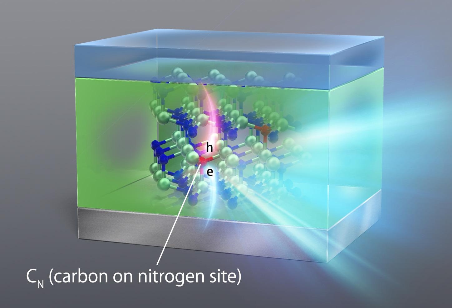
Scientists find impurities to be at the heart of the poor performance of semiconductors. Carbon impurities in gallium nitride (GaN) semiconductors affect GaN crystal growth and degrade their performance. Image Credit: Masashi Kato from Nagoya Institute of Technology.
A curious experimental manifestation of deep levels is the appearance of a long-lived yellow luminescence in the photoluminescence spectrum of GaN along with a long charge carrier recombination time reported by characterization techniques like time-resolved photoluminescence (TR-PL) and microwave photoconductivity decay (µ-PCD). However, the mechanism underlying this longevity is unclear.
In a recent study published in the Journal of Applied Physics, scientists from Japan explored the effect of deep levels on the yellow luminescence decay time and carrier recombination by observing how the TR-PL and µ-PCD signals changed with temperature. “Only after understanding the impacts of impurities in GaN power semiconductor devices can we push for the development of impurity control technologies in GaN crystal growth,” says Prof. Masashi Kato from Nagoya Institute of Technology, Japan, who led the study.
The scientists prepared two samples of GaN layers grown on GaN substrates, one doped with silicon and the other with iron. The unintentional doping of carbon impurities happened during the silicon doping process. For the TR-PL measurements, the team recorded signals for temperatures up to 350°C while for µ-PCD up to 250°C due to system limitations. They used a 1 nanosecond-long UV laser pulse to excite the samples and measured the reflection of microwaves from the samples for µ-PCD.
The TR-PL signals for both samples showed a slower (decay) component with a decay time of 0.2–0.4 milliseconds. Additionally, the use of a long-pass filter with a cut-off at 461 nm confirmed that yellow light was involved. In both samples, and for both TR-PL and µ-PCD measurements, the decay time declined above 200°C, consistent with previous reports.
To explain these findings, the scientists resorted to numerical calculations, which revealed that the deep levels essentially trapped “holes” (absence of electrons) that eventually recombined with free electrons but took long to do so due to the extremely small chance of an electron being captured by the deep level. However, at high temperatures, the holes managed to escape from the trap and recombined with the electrons through a much faster recombination channel, explaining the decline in decay time.
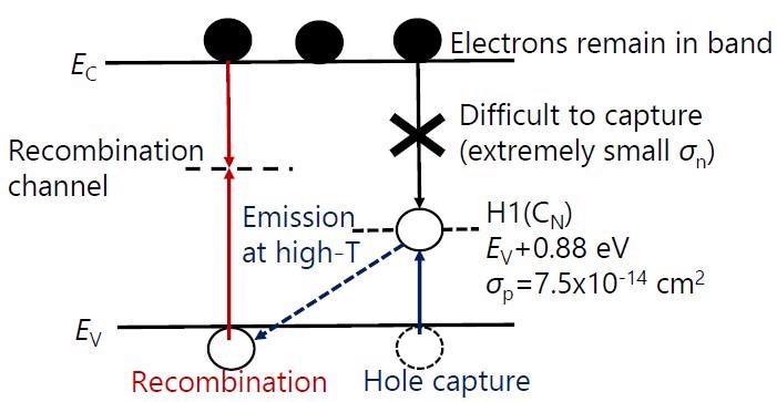
An analytical model based on energy band representation was proposed to explain the temperature dependence of the time constants in the TR-PL and µ-PCD decay curves
At low temperatures, holes are trapped in H1 and take long to recombine with electrons in EC due to difficulty in electron capture. At high temperatures, the holes escape to EV and recombine with electrons through the recombination channel. Image Credit: Masashi Kato from Nagoya Institute of Technology
“To reduce the effects of the slow decay component, we must either maintain a low carbon concentration or adopt device structures with suppressed hole injections,” says Prof. Kato.
With these insights, it is perhaps only a matter of time before scientists figure out how to avoid these pitfalls. But with GaN’s rise to power, will it be just better electronics?
Prof. Kato thinks otherwise. “GaN enables lower power losses in electronic devices and therefore saves energy. I think it can go a long way in mitigating greenhouse effects and climate change,” he concludes optimistically. These findings on impurities may thus be what lead us to a cleaner, greener future.
Reference
Title of original paper: Contribution of the carbon-originated hole trap to slow decays of photoluminescence and photoconductivity in homoepitaxial n-type GaN layers
Journal: Journal of Applied Physics
DOI: https://doi.org/10.1063/5.0041287