Through a solid-state process of diffusion, FeCoB nanocrystal films (Fe:Co:B=60:20:20 at atom ratio) permit dimensional lattice targeted, microstructurally diamond elimination.
Importance of Diamond
Diamond has distinct biochemical and visual qualities in addition to its high elasticity and toughness. Its extreme durability is a vital source for advancements in ultraprecision processing (diamond turning techniques) and a road to extreme pressures in the hundreds of GPa range.
Chemical impermeability, visual durability, and bioactivity have expanded the system design for utilizing these functional qualities. Diamond has carved out a place for itself in Mechatronics, optical components, sensing, and data management.
Patterning of Diamond
To allow their applications, the incorporation of diamond and its patterning presents distinct problems. Reactive ion etching (RIE), inductively coupled plasma (ICP), and electron beam induced etching are examples of existing process systems that use etching-based technologies (EBIE).
The diamond structure has also been created using laser and focused ion beam (FIB) machining techniques. The goal of such manufacturing engineering has been to speed up delamination while also allowing for scalability across broad regions within a sequential manufacturing structure. Fluidic etchants (plasma, gaseous, and liquid solution) are used in these procedures, which limits the geometrical sophistication that may be achieved.
Substance ablation of chemical vapor produced, polycrystalline diamond utilizing FeCoB (Fe:Co:B at 60:20:20 atomic percent) designs on its surfaces was investigated in this innovative work. The focus is on patterning the TM to precisely etch m-scale structures in diamonds. The underlying diamond is coupled with nanocrystal FeCoB by thermal treatment at temperatures ranging from 700 °C to 900 °C for 30 minutes to 90 minutes.
Surface Roughness Results
The original layer of the diamond specimens was indicative of the underlying fundamental polycrystalline microstructures. Within each particular particle, the roughness (Ra) was 3.84 ± 0.47 nm, whereas the total roughness of the surface was 9.6 ± 1.2 nm. The roughness (inside one diamond grain) of the implanted FeCoB metal layer was 3.39 ± 0.26 nm, while the layer's height was 100 ± 10 nm.
The thickness of the metallic surface grew to 600 ±100 nm after 30 minutes of annealing at 800 °C, while the roughness (Ra) of the surface climbed to 224 ± 22 nm. During the annealing operations, carbon atoms diffuse into the FeCoB layers, leading to an increase in dimension.
Etching Rate Analysis
3 specimens with a 100 nm thick FeCoB layer were heated at temperatures of 700 °C, 800 °C, and 900 °C, respectively. When the temperature range is below 700 °C, no substantial engagement between diamond and FeCoB occurs, and very minor material removal happens following the hydrothermal method treatment. The material removal is enhanced to temperatures above 800 °C.
When the temperatures hit 900 °C, the etching rates were twice as fast as when the temperatures were 800 °C. However, the etched area's profile differs greatly from the implanted etchant sequence (FeCoB).
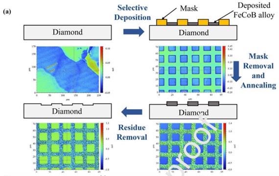
Schematic showing visualization of Solid State Etchants for pattern creation Study: Spatially selective, solid-state etching of diamond using lithographically patterned FeCoB. Image Credit: Wang, Z. & Shankar, M. R. et al., Diamond & Related Materials
Etching Depths
The 100 nm FeCoB on the diamond specimens were treated at 800 °C for 30 minutes, 60 minutes, and 90 minutes, respectively.
With time, the etching depth grew linearly.
At 800 °C, the engraved area's roughness (Ra) was determined as a function of response time. The hardness of the sample after 30 minutes, 60 minutes, and 90 minutes annealing was 186 ±28 nm, 203 26 nm, and 212 30 nm, respectively. When the etching depth is 500 nm, 800 nm, or 100 nm, the engraved area ruggedness to etching depth ratio (RD) is 0.372, 0.254, and 0.212, respectively.
The etched area's roughness did not considerably enhance as the etching depth was increased. The temperatures necessary to initiate the reactions between the diamond and the TM etchant were discovered to be greater than 700 °C.
The findings indicated that FeCoB enables effective diamond removal at a pace that is substantially faster than Fe or Co alone.
By tweaking the structure and morphology of the FeCoB, a prospective method for retaining the effective diamond extraction and boosting the selectivity of the material removal arises.
Challenges
The ability to achieve surfaces of predictable topographic grade is a fundamental issue in transferring the utility of solid-state alkaline solutions into scaling foundations for manufacturing micro/nanostructured diamond substrates. It's crucial to pinpoint where the diamond and TM interact inside the interface region.
To summarize, solid-state programming of polycrystalline diamond surfaces is possible thanks to geographically controlled C diffusion across diamond-FeCoB surfaces. At temperatures over 800 °C, lithographically etched transition metal coatings expedite the elimination of C from diamond. This technique could further be studied to enhance stability and etching rates.
References
Wang, Z. & Shankar, M. R., 2021. Spatially selective, solid state etching of diamond using lithographically patterned FeCoB. Diamond & Related Materials. 108763. Available at: https://www.sciencedirect.com/science/article/pii/S0925963521005264?via%3Dihub
Disclaimer: The views expressed here are those of the author expressed in their private capacity and do not necessarily represent the views of AZoM.com Limited T/A AZoNetwork the owner and operator of this website. This disclaimer forms part of the Terms and conditions of use of this website.