Image Credit: © Imperial College London.
Silicon chips are the components that drive the majority of daily electronics, from smartphones to fitness trackers. However, their inflexible nature restricts their use in flexible electronics. Composed of single-atom-thick layers, 2D materials can be spread in solution and formulated into printable inks, creating ultra-thin films that are very flexible, semi-transparent and with unique electronic properties.
This paves the way for the possibility of new types of devices, such as those that can be combined with stretchable and flexible materials, like clothes, paper or even tissues into the human body.
Controlled Design and Engineering
Earlier, scientists have fabricated numerous flexible electronic devices from printed 2D material inks, but these have been limited-edition ‘proof-of-concept’ components, constructed to exhibit how one specific property, such as light detection, high electron mobility or charge storage can be achieved. However, without ascertaining which parameters to regulate in order to build printed 2D material devices, their extensive use has been limited.
Currently, the international team of researchers has analyzed how an electronic charge is conveyed in a number of inkjet-printed films of 2D materials, showing how it is regulated by variations in temperature, electric field and magnetic field.
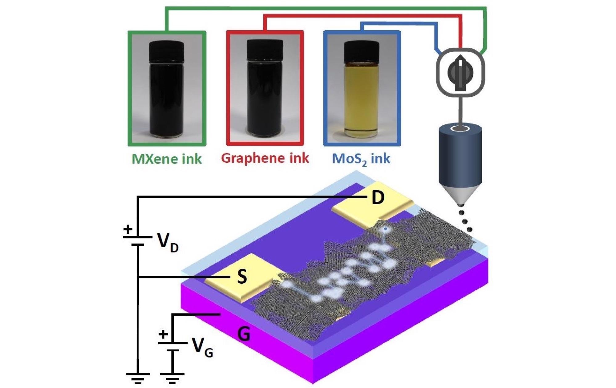
The researchers explored three standard types of 2D materials: molybdenum disulfide (or MoS2, a ‘semiconductor’), graphene (a ‘semimetal’ built from a single layer of carbon atoms) and titanium carbide MXene (or Ti3C2, a metal) and mapped how the behavior of the electrical charge transport altered under these diverse conditions.
These future devices could someday substitute invasive procedures, such as implanting brain electrodes to track degenerative conditions that impact the nervous system. Electrodes can only be implanted on a short-term basis and cause discomfort for the patient, whereas a flexible device created using biocompatible 2D materials could be incorporated with the brain and offer continuous monitoring.
Our results have a huge impact on the way we understand the transport through networks of two-dimensional materials, enabling not only the controlled design and engineering of future printed electronics based on 2D materials, but also new types of flexible electronic devices.
Dr. Felice Torrisi, Study Lead, Department of Chemistry, Imperial College London
“For example, our work paves the way to reliable wearable devices suitable for biomedical applications, such as the remote monitoring of patients, or bio-implantable devices for long-term monitoring of degenerative diseases or healing processes,” Dr. Torrisi added.
Other possible healthcare applications include wearable devices for tracking healthcare – devices such as fitness watches, but more cohesive with the body, delivering adequately accurate data to permit doctors to track patients without having to bring them into hospital for tests.
Optimal Designs
The team found the relationships between 2D material type and the controls on electrical charge transport, which would help other scientists engineer printed and flexible 2D material devices with the properties they prefer, based on how they need the electrical charge to behave.
They could also reveal how to develop totally new types of electrical components that were impossible using silicon chips, such as transparent parts or ones that adapt and convey light in new ways.
The fundamental understanding of how the electrons are transported through networks of 2D materials underpins the way we manufacture printed electronic components. By identifying the mechanisms responsible for such electronic transport, we will be able to achieve the optimum design of high-performance printed electronics.
Professor Renato Gonnelli, Study Co-Author, Politecnico di Torino, Italy
Co-first author Adrees Arbab, from the Department of Chemistry at Imperial and the Cambridge Graphene Centre, stated “In addition, our study could unleash the new electronic and optoelectronic devices exploiting the innovative properties of graphene and other 2D materials, such as incredibly high mobility, optical transparency, and mechanical strength.”
Journal Reference:
Piatti, E., et al. (2021) Charge transport mechanisms in inkjet-printed thin-film transistors based on two-dimensional materials. Nature Electronics. doi.org/10.1038/s41928-021-00684-9.