The first step involved the use of a low-intensity ultraviolet-ozone (UVO) radiation to oxidize mechanically exfoliated BP flakes followed by an argon (Ar) plasma treatment, which removed the oxidized layer and thinned BP flakes. In the second step, the thinned BP flakes were annealed to reduce surface impurities and defects, post-radiation and Ar treatment.
Due to low damage and effective control of BP flake thickness, electronic semiconductor devices such as field-effect transistors demonstrated higher efficiency.
BP Flakes and its Applications
BP flake is one of the most promising 2D semiconductor materials that exhibit properties such as a thickness-dependent bandgap, extraordinary thermoelectric properties, high carrier mobility, enhanced optoelectronic properties, and improved biomedical performance.
However, the lack of a suitable low-cost and energy-efficient thin-film fabrication process and surface degradation after the thinning process limits its practical applications. Thinning processes used for BP flakes include wet chemical and thermal treatment, conductive atomic force microscope anodic oxidation and electron beam sculpting, and thermal oxidization and plasma treatment.
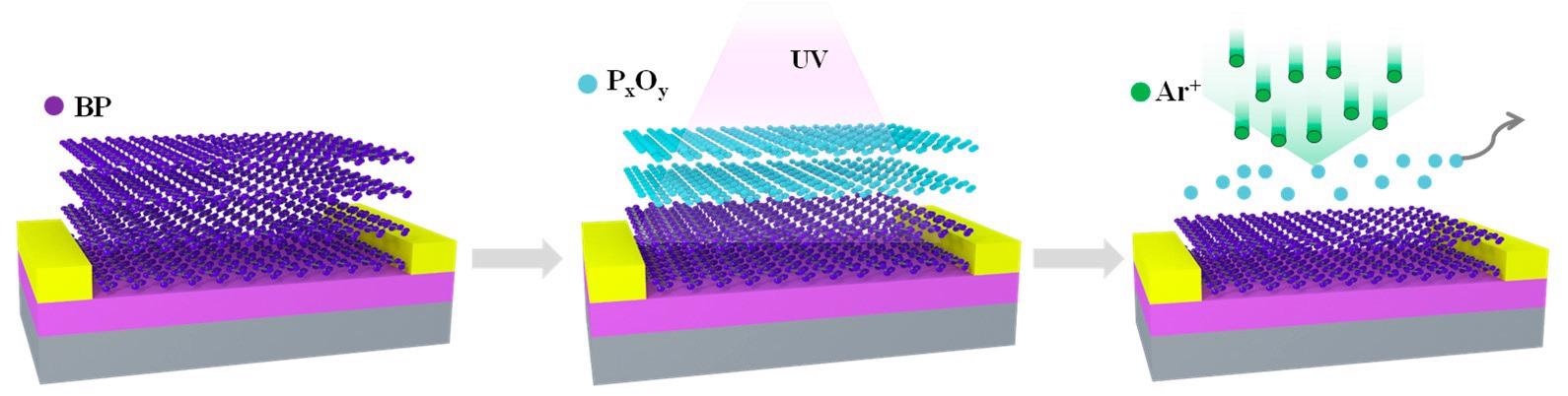
Schematic diagram of thinning process of the BP flakes. Slight UVO radiation was introduced to oxidize the BP flakes, and Ar plasma was used to remove the residue. Image Credit: Lu, Q et al., Materials
UVO radiation is one of the widely used thermal oxidization processes owing to the formation of a more stable BP surface, whereas Ar plasma treatment is used to remove the oxidized residues, but these two processes influence the electronic performance of devices due to the formation of surface defects, and subsequent ununiform surface oxidization.
As simple UVO radiation and Ar plasma treatment are not enough to achieve a stable thinning rate of exfoliated BP flakes, a secondary annealing process can be incorporated.
About the Study
In this study, researchers first procured BP flakes from mechanical exfoliation of a bulk BP crystal by Scotch tape. The obtained BP flakes were then exposed to a low-intensity UVO radiation of 50 watts, which resulted in a BP flake thinning rate of about 2 nm/min due to the ozone oxidation without direct bombardment.
Subsequently, an Ar atmosphere plasma beam was introduced using a reactive ion etching (RIE) equipment to remove the oxidized residue on the top surface of the BP followed by a 300 °C annealing process for 1 min in nitrogen (N2) atmosphere to eliminate the interface defects.
Subsequently, the thinned BP flakes were characterized using an optical microscope, an atomic force microscope (AFM) in tapping mode, a Raman spectrometer with an excitation wavelength of 514 nm, and an X-ray photoelectric spectroscopy (XPS) to analyze the binding energies of the BP flakes. Finally, they were used to fabricate a field-effect transistor (FET) whose performances were calibrated using a semiconductor parameter analyzer under vacuum conditions.
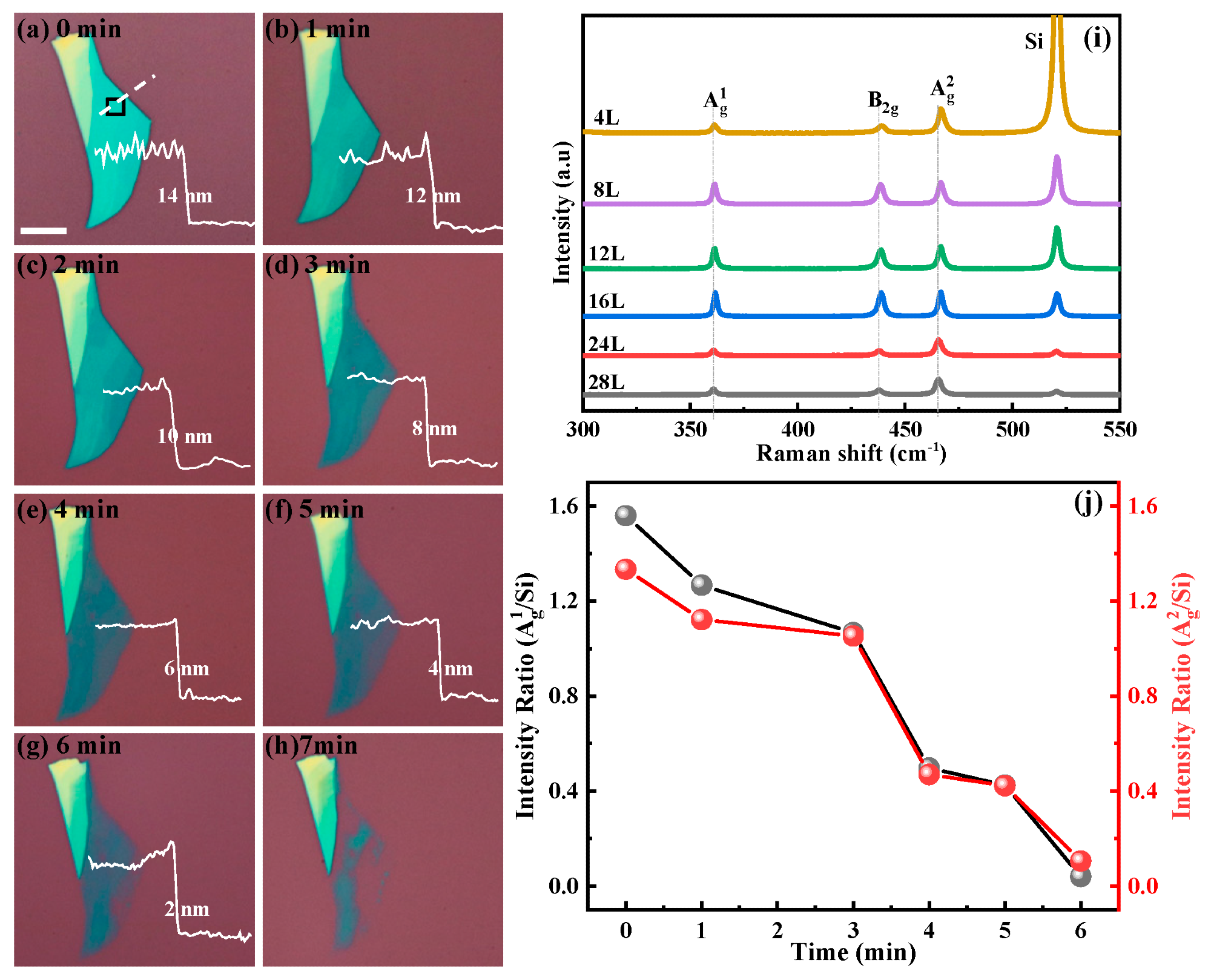
Optical images of mechanically exfoliated BP flakes treated with UV light radiation at different times and 300 °C annealing in N2 atmosphere (a–h). The length of the scale bar is 5 μm. Thinned thicknesses of BP flake as a function of the radiation time are shown as white lines. (i) Raman spectra of the BP flake being treated for various UVO light radiation corresponding to (a–g). (j) Intensity ratio of the A1g/Si and A2g/Si as functions of the UVO light radiation time. Image Credit: Lu, Q et al., Materials
Observations
Some small bubbles were observed on the surface of BP flake in optical microscopy and AFM images due to residual airborne H2O and O2, even under vacuum conditions. The thickness of the prepared thinned BP flake sample was ~8 nm, compared with a thickness of ~13 nm before thinning. Similarly, the measured surface roughness of the thinned BP flakes was 1.76 nm, compared with 1.73 nm before thinning, which was a very minor increase. This could be due to the use of a high-power laser during the Raman test.
Raman spectroscopy showed that the thinning rate was about 2 nm/min from an initial thickness of 14 nm. Also, the three prominent spectra peaks at 360.7, 437.4, and 465.6 cm−1, both before and after the UVO radiation treatment, were attributed to the vibration of the crystalline lattice of BP viz. the A1g (out-of-plane vibrations), B2g, and A2g (in-plane vibrations) phonon modes. This indicated the retaining of the crystallinity of BP after UVO light and plasma treatment.
The XPS spectrum showed constant binding energy of 284.6 ± 0.2 eV. Before thinning treatment, the decomposition of the phosphor into two peaks located at ~129.9 and 130.8 eV was assignable to 2p3/2 and 2p1/2 binding energy, respectively. The broad bulging located at ~134 eV was due to the oxidation BP and formation of P-O-P, O-P=O, and P2O5 bonds during the treatment process. Moreover, after the annealing, the peak intensity corresponding to 134 eV decreased due to the partial reduction of oxygen during the thinning process.
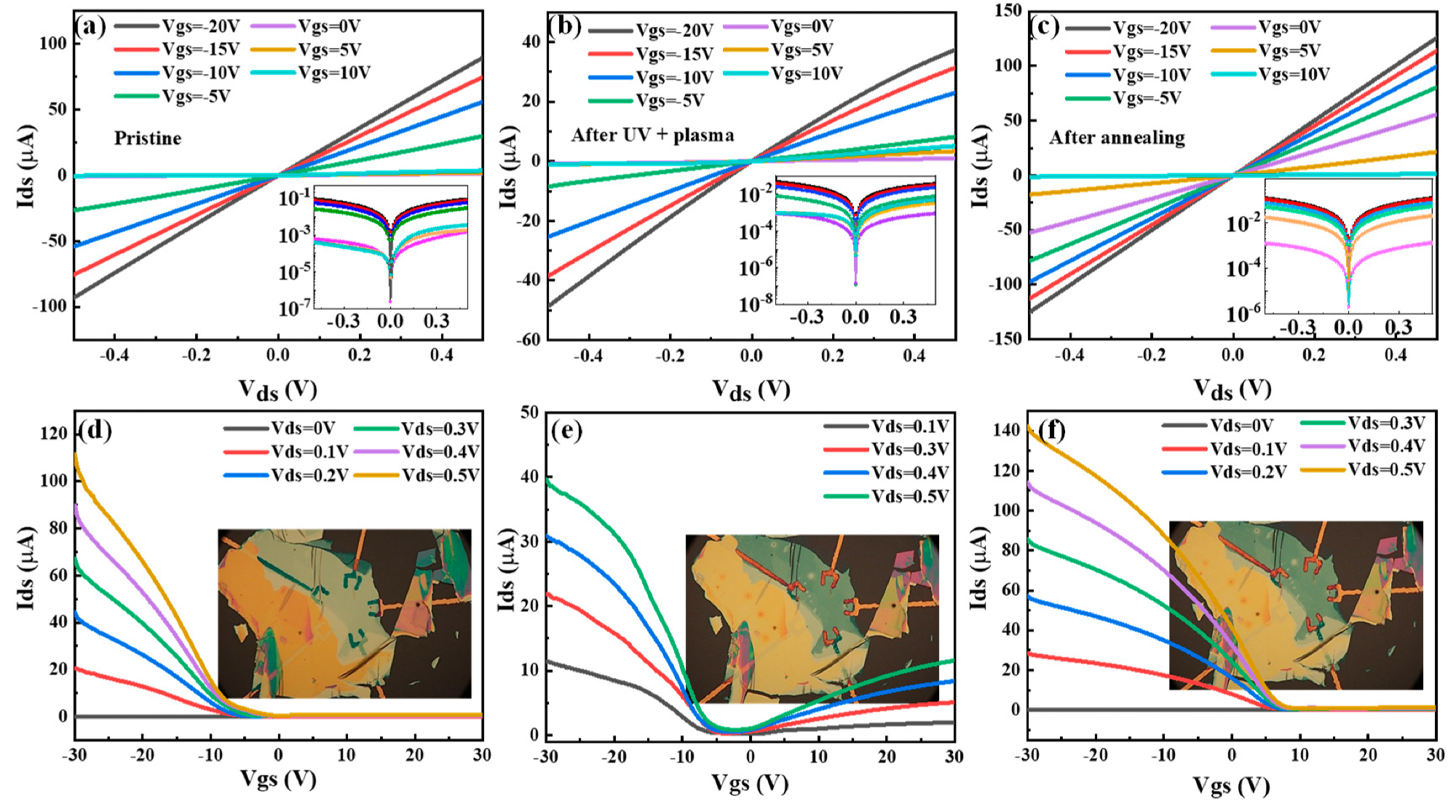
Current performance of BP flakes under different status which were tested at room temperature. Ids-Vds characteristics of BP FET at pristine (a), after thinning by 5 min light UVO and slight Ar+ plasma treatment (b), and after 300 °C annealing in N2 atmosphere (c), with Vgs varying from -20 V to 10 V. Insets are log-scale plots with unit A on the y-axes. Ids-Vgs characteristics at pristine (d), after UVO and Ar+ plasma treatment (e), and after annealing (f), with Vds varying from 0 V to 0.5 V. The insets are optical microscopy images of fabricated BP FETs under different treatments. Image Credit: Lu, Q et al., Materials
Conclusions
Researchers fabricated desired thin BP flakes using a two-step process. Firstly, they used a low-intensity UVO radiation to oxidize the BP flake surface and thin it followed by using an Ar plasma treatment to remove any remaining residues. After that, those flakes were annealed at a temperature of 300 °C in an N2 atmosphere to eliminate any surface defects.
The prepared thinned BP flakes were further used to fabricate an FET, which demonstrated high efficiency. Thus, this two-step thin BP flake fabrication process is a simple, cost-effective, and minimal waste process for BP-based high-performance semiconductor devices.
Reference
Lu, Q., Li, X., Chen, H., Jia, Y., Liu, T., Liu, X., Wang, S., Fu, J., Chen, D., Zhang, J., Hao, Y., Study on Black Phosphorus Characteristics Using a Two-Step Thinning Method. Materials, 2022, 15, 615. https://www.mdpi.com/1996-1944/15/2/615
Disclaimer: The views expressed here are those of the author expressed in their private capacity and do not necessarily represent the views of AZoM.com Limited T/A AZoNetwork the owner and operator of this website. This disclaimer forms part of the Terms and conditions of use of this website.