They are easily manufactured using electron beam lithography, nano-imprinting, self-organization, or three-dimensional (3D) printing. The layered or 3D structured pattern of metamaterials makes them capable of matching the free space impedance and the fabrication of passive EM devices such as filters, collimators, lenses, perfect absorbers, polarizers, attenuators, and bolometers.
The addition of graphene in the form of a one-atom-thick graphite layer in metamaterials allows for perfect and tunable THz absorption because it absorbs 2.3% of light at optical frequencies interband transitions.
In the present study, researchers proposed a tool for designing and manufacturing graphene-enhanced passive devices developed on gold-plated patterned dielectric substrates. Furthermore, they investigated the effect of non-homogeneity and roughness of the gold thin film on THz performance and also used the Drude–Smith model for gold conductivity simulation of experimentally observed THz response oscillations.
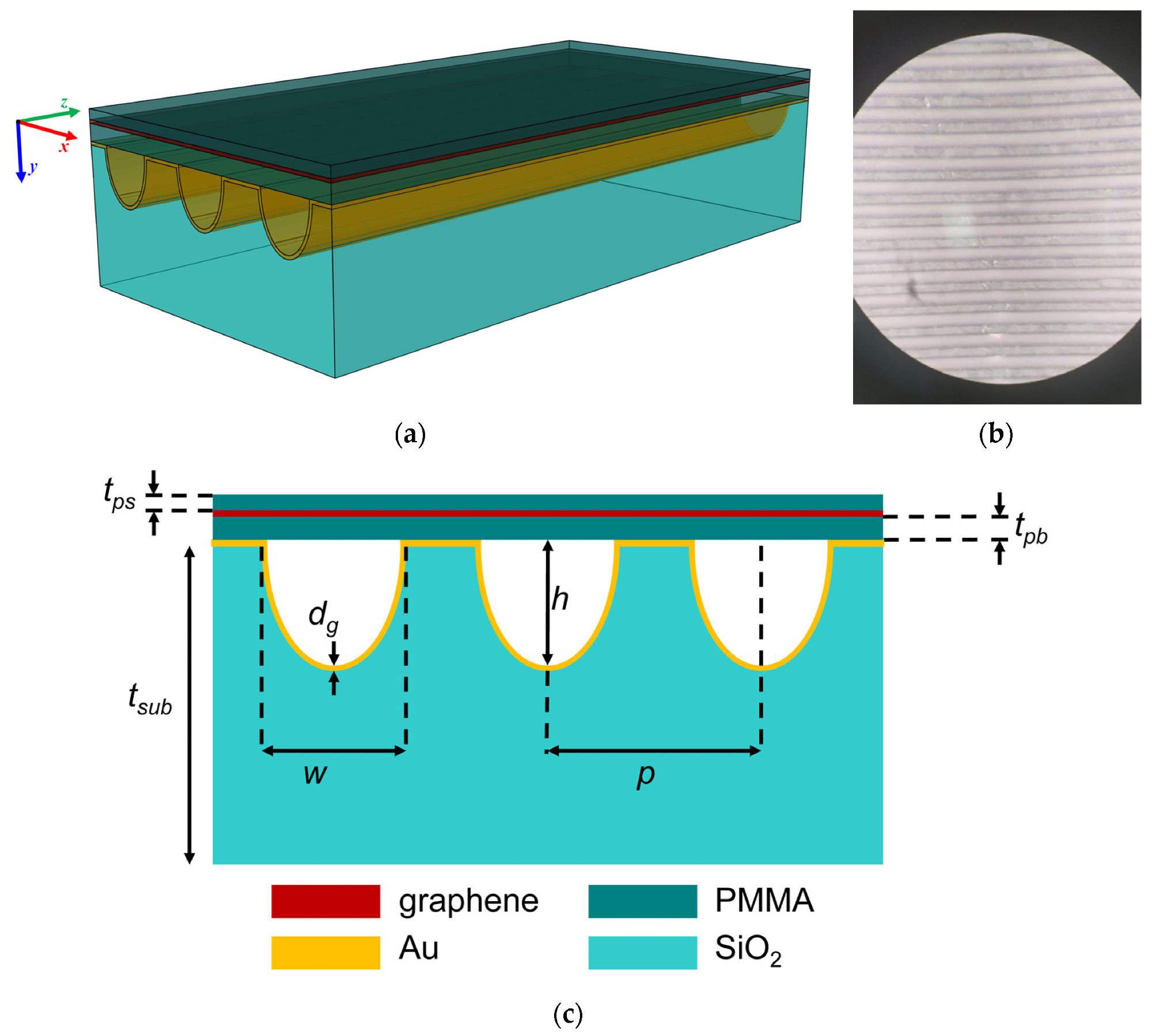 (a) Three-dimensional sketch of the graphene/gold/patterned SiO2 metasurface. (b) Photo of the top view of the graphene/gold/SiO2 patterned metasurface. (c) Cross-section of the metasurface. Image Credit: Lamberti, P. et al., Materials
Methodology
For graphene/gold/patterned SiO2 metasurface fabrication, THz grating was made on a fused silica SiO2 substrate using femtosecond micromachining and conventional chemical vapor deposition (CVD) methane-based process, and the graphene was grown on a Cu foil. A sputtering instrument was used to deposit a gold conductive layer on the micromachined substrate. After that, the resulting samples were baked for 10 minutes at 60 degrees celsius, and graphene from the other side of the Cu foil was removed using oxygen plasma treatment.
Commercial finite element method (FEM) software was used to model THz's fabricated structure. In the FEM model, the graphene/gold/patterned SiO2 metasurface structure can be assumed to be infinite in the longitudinal direction, reducing the problem to a two-dimensional model. Additionally, the distance between both ports of the FEM model was assumed to be much longer than the EM wavelength.
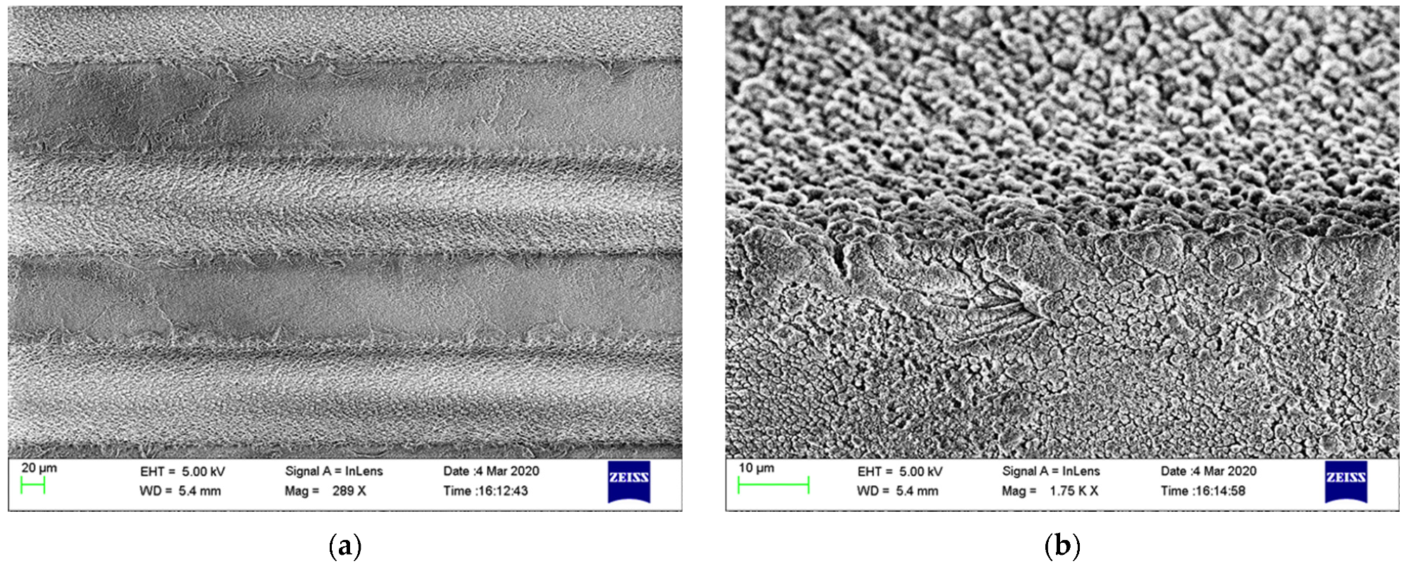
(a,b) SEM images of patterned SiO2/gold diffraction grating, where (b) demonstrates the groove interface. (c) AFM of the plane SiO2 surface covered with gold. (d) Raman spectra of CVD graphene used for metasurface fabrication. Image Credit: Lamberti, P. et al., Materials
Results
The scanning electron microscope and atomic force microscopy images of graphene/gold/patterned SiO2 metasurface showed that the patterned SiO2 had a rough and porous surface due to the femtosecond micromachining. This is because of the higher deposition of the gold thickness and its sheet conductivity, as the surface area of the patterned substrate is higher than the graphene/gold/patterned SiO2 metasurface sample, which was not micromachined.
The FEM numerical simulation revealed how the THz performance is influenced by metasurface geometry and provides guidelines for designing a best-performing and robust configuration. Additionally, the FEM numerical simulation was also used in this study to determine the effect of the gold reflector layer conductivity on overall device performance.
Considering the asymmetry of the carriers scattering in the thin metal film, the FEM numerical simulation revealed the impact of the gold layer imperfection on the THz performance.
The Drude–Smith model described the measured spectra of the transmission, absorption, and reflection of the SiO2 grating covered by the deposited thin gold film. The model also described the Fabry–Pérot interference pattern and other EM features present in the metasurface's experimental behavior, allowing for further investigation of metasurface's performance in various applications.
Furthermore, the current study results showed that the predominant backscattering of the carriers in the thin film affects the THz properties of the gold layer and significantly impacts the performance in the frequency range of interest.
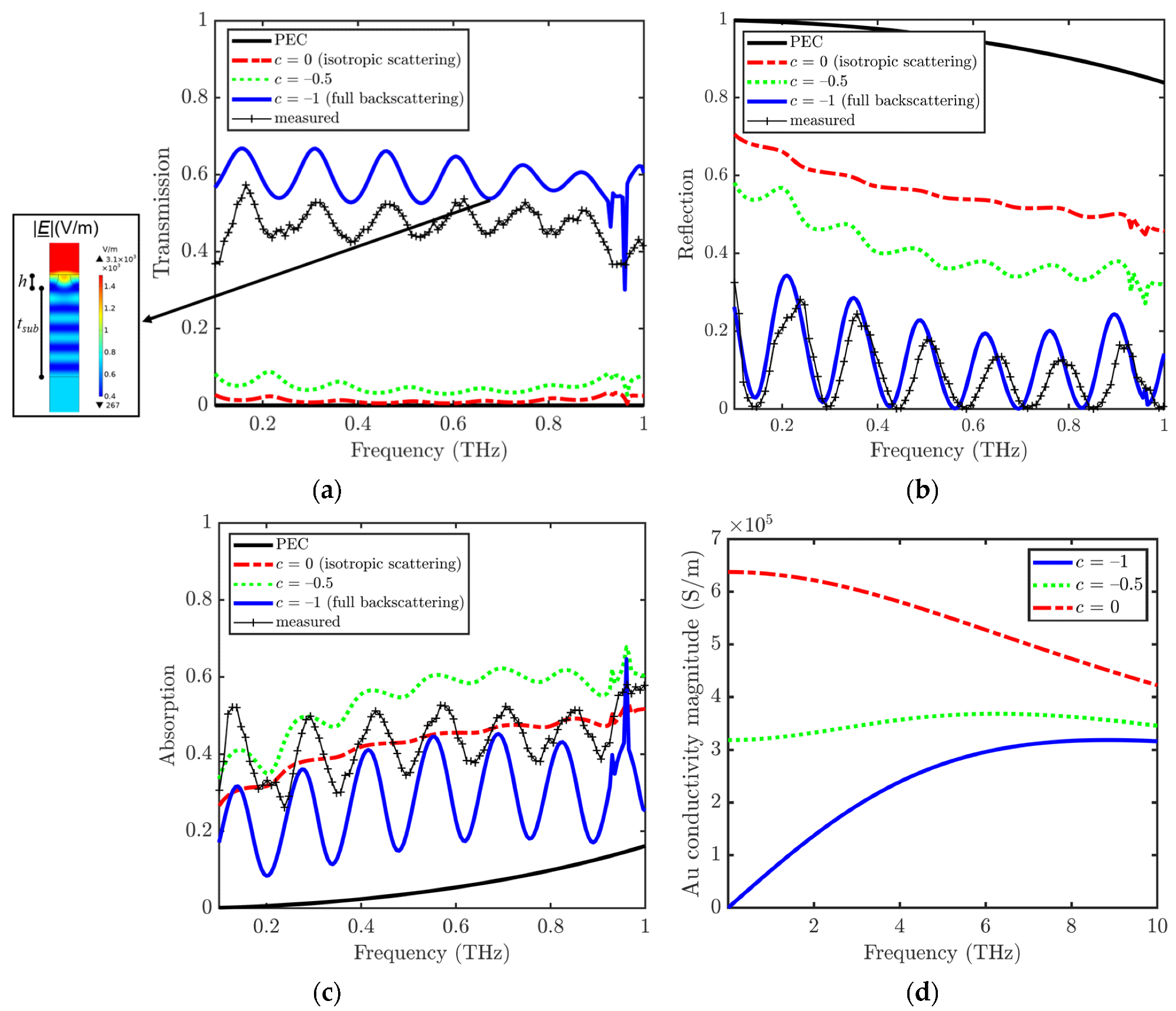
Simulated power (a) transmission, (b) reflection, and (c) absorption spectra of the graphene/gold/patterned SiO2 metastructure computed by FEM simulations, at different c corresponding to different conditions of gold nonideality, exciting the top port with a THz electric field parallel to the grooves and normally incident on the device top surface, in the frequency range of 0.1–1 THz. (d) The magnitude of the gold layer complex conductivity in the frequency range 0.1–1 THz. Inset of (a): electric field magnitude distribution in the cross-section surface at f = 0.685 THz, in correspondence with a minimum of T and R and a maximum of A. In order to evidence the grooves’ location, h and tpb parameters are also reported here. Image Credit: Lamberti, P. et al., Materials
Conclusions
The current work was aimed at improving the overall absorption in the metasurface using grating cavities in graphene. The grating has the unique effect of diffracting rather than simply reflecting the incident wave because of which the energy of the radiating source is spread out in different directions. As a result, multiple reflections between the grating cavities and the graphene layer are triggered, improving the overall absorption.
The numerical simulation results revealed the effect of the gold layer's imperfection on the THz metasurface's performance, while the Drude–Smith model of metal conductivity accurately described the experimental results considering the anisotropic scattering of carriers in thin metal films.
According to the researchers, the metasurface's THz performance can significantly improve if a different physical deposition technique such as thermal vacuum deposition electroplating is used for manufacturing.
Disclaimer: The views expressed here are those of the author expressed in their private capacity and do not necessarily represent the views of AZoM.com Limited T/A AZoNetwork the owner and operator of this website. This disclaimer forms part of the Terms and conditions of use of this website.
Source:
Lamberti, P.; La Mura, M.; Tucci, V.; Nkyalu, E.; Khan, A.; Yakovleva, M.; Valynets, N.; Paddubskaya, A.; Saushin, A.; Vanyukov, V.; et al. The Performance of Graphene-Enhanced THz Grating: Impact of the Gold Layer Imperfectness. Materials 2022, 15, 786. https://www.mdpi.com/1996-1944/15/3/786/htm