Performance Improvement of Metal Halide Perovskites
Silicone-based single-junction solar cells have shown the highest PCE value up to 32% owing to their lowest bandgap of 1.1 eV, which is close to the Shockley–Queisser limit of 33.16%. Meanwhile, metal halide perovskites (ABX3) such as CsPbBr3, CsPbCl3, and CsPbI3, are an emerging class of photovoltaic (PV) ceramics with flexible structure and tunable bandgap to absorb solar irradiation of a wide range of wavelengths. In just the last decade, their PCE has gone up from 2% to 25% Thus, flexible perovskite solar cells (FPSCs) in tandem with silicone can achieve both high PCE with a tunable absorption spectrum.
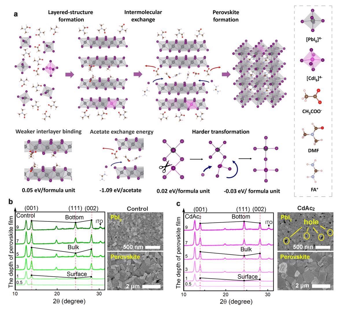
Schematic formation of nano-hole array PbI2 and FAPbI3 films. (a) Illustration of thin-film growth mechanism for the perovskite with and without the addition of CdAc2. (b) and (c) GIXRD of perovskite films without and with CdAc2, the angles varied from 0.5o to 9o (inset image: surface-sectional SEM images of PbI2 films and perovskite films). Image Credit: Ren, N et al., Research Square
However, the primary issue with metal halide perovskite solar cells (MHPSCs) is that their flexible crystalline film structure strongly depends on a flexible substrate which influences the number of nucleation sites, crystal growth rate, and crystal orientation.
A rough substrate means more defects in the perovskite film; on top of that, thermal expansion coefficient mismatch between the substrate and perovskite film leads to high defect density. Currently, the most commonly used substrates for perovskite films are polyethylene terephthalate (PET) and polyethylene naphthalate (PEN); both suffer from high surface roughness and thermal shrinkage.
About the Study
In this study, researchers added CdAc2 in the PbI2 perovskite precursor ink solution to manipulate the perovskite nucleation density and crystal growth, resulting in enhanced optoelectronic properties on the perovskite/silicone TSC with a flexible substrate and textured silicon substrate. Subsequently, they performed density functional theory (DFT) measurements to study the intermolecular interaction of CdAc2 with PbI2.
The FPSC was based on FAPbI3, which was fabricated using a two-step solution method. The pinholes formed due to the introduction of CdAc2 facilitated the diffusion and intercalation of the ammonium cation that resulted in large and uniform FAPbI3 grains.
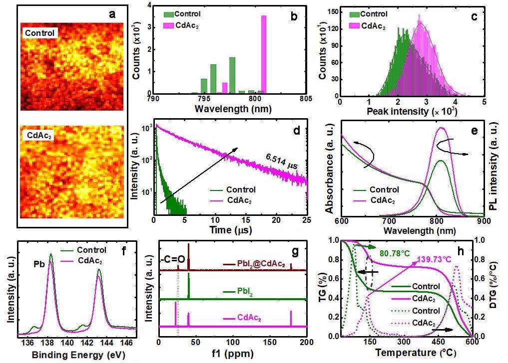
Characterization of the FAPbI3 films on flexible PET/ITO substrates. The photoluminescence (PL) (a) mapping and (b) peak position of perovskite films prepared with or without CdAc2 (region size: 20 x 20 mm). (c) Histograms of PL peak position (extracted from PL mapping data) of perovskite films prepared with or without CdAc2. (d) Time-resolved photoluminescence of the FAPbI3 films. (e) UV–vis absorption and PL spectra of the FAPbI3 films. (f) XPS core-level spectra of Pb on perovskite films prepared with or without CdAc2. (g) 13C solution-state NMR spectra of Precursor PbI2 solution. (h) TGA curve of precursor PbI2 solution with and without CdAc2. Image Credit: Ren, N et al., Research Square
Observations
The DFT results confirmed that the CdAc2 coordinated with PbI2 to form an intermediate phase and decrease the FAPbI3 crystal growth rate, which resulted in an enhanced crystallinity of the fabricated perovskite film. Also, the crosslinking of Ac-ions passivated the FAPbI3 grain boundaries, which led to the improved thermal stability of the FAPbI3 film. Moreover, the intrinsic defect density of FAPbI3 polycrystalline thin film was significantly reduced that increasing the carrier lifetime to over 6 μs. Higher carrier lifetime means higher current density and higher PCE.
Furthermore, during the reactions between FAI and Ac2 ion-doped PbI2 films, the Ac-ion was replaced by I-ion to produce a smooth PbI2 surface. The induction of Cd in the FAPbI3 lattice increased the activation barrier for the reaction, which converted the layered structure into a 3D perovskite structure. This led to a damped crystallization process and resulted in larger and uniform perovskites grains.
The time-resolved photoluminescence (TRPL) results showed that the longer carrier lifetime (>6 μs) of CdAc2-treated FAPbI3 perovskite film suppressed the non-radiative recombination process, which is a major source of PCE loss in single-junction solar PV cells.
In the end, the fabricated CdAc2 added FAPbI3 /silicone TSC demonstrated a PCE of 29.25% and 23.07% for an aperture area of 0.5003 cm2 and 11.8792 cm2, respectively, with efficiency retention of 109.78% of their initial value continuous one-sun illumination at 45 oC in N2 atmosphere after 300 hours.
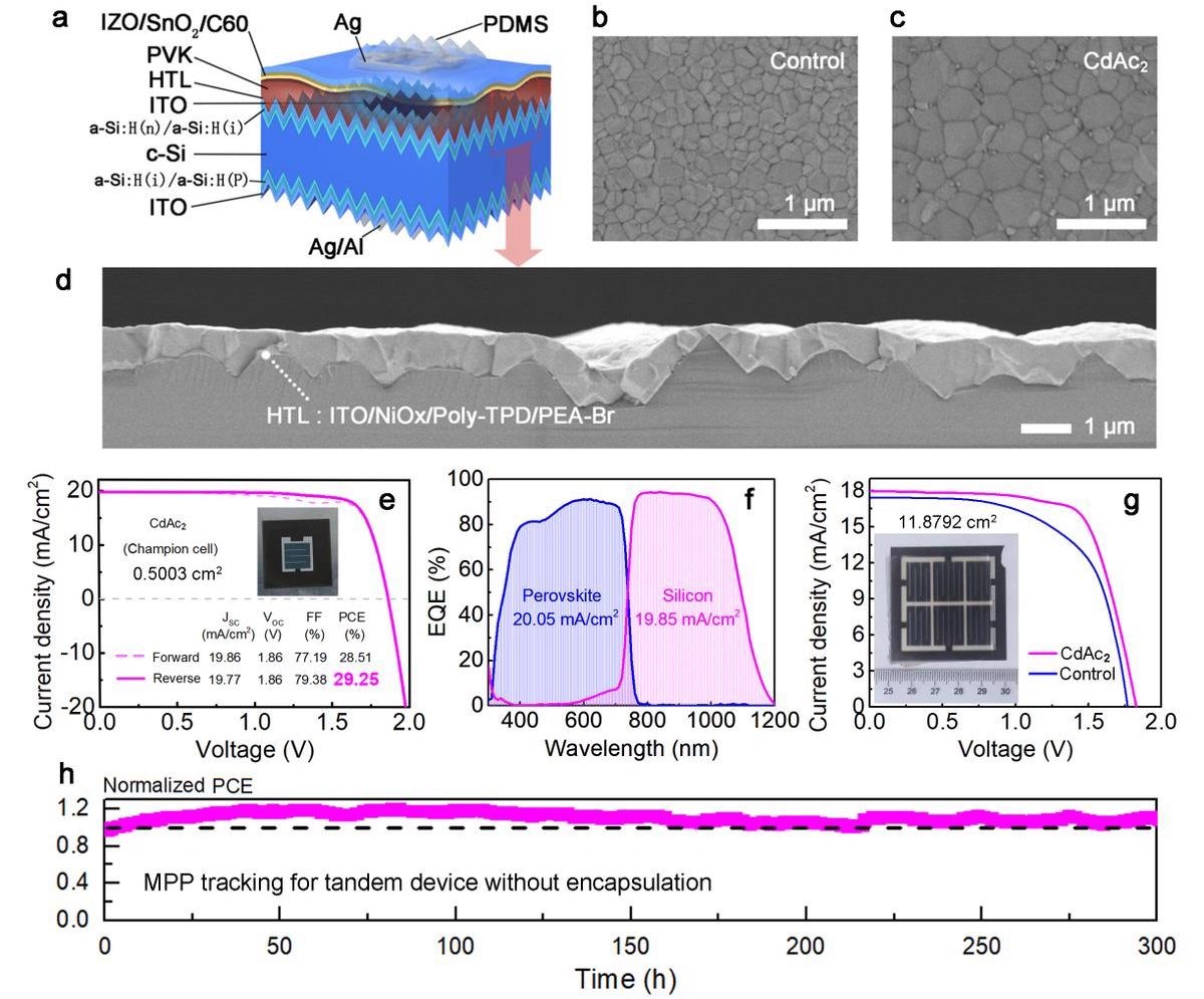
Characteristics of monolithic perovskite/silicon tandem solar cells based on textured substrate using CdAc2. (a) Schematic stack of the monolithic perovskite/silicon tandem solar cell. SEM top-view image of solution-processed perovskite film without (b) and with (b) CdAc2. (d) SEM cross-section image of a textured c-Si with an average pyramid size of 2 µm (e) J-V characteristics of tandem solar cells without and with CdAc2 with an effective area of 0.5003 cm2. The illustration is the photo of a complete tandem device. (f) The EQE of the tandem device with CdAc2 treatment. (g) J-V characteristics of tandem solar cells without and with CdAc2 with an effective area of 11.8792 cm2. The illustration is a photo of a complete tandem device. (h) Mpp tracking for TSCs without encapsulation. Image Credit: Ren, N et al., Research Square
Conclusions
In summary, the researchers of this study fabricated CdAc2-doped PbI2 perovskite precursor ink solution for FAPbI3 /silicone TSC. The Cd inserted FAPbI3 lattice resulted in a 3D perovskite structure with larger and uniform perovskites grains, improved thermal stability, suppressed non-radiative recombination, improved the carrier lifetime, and enhanced PCE over a tunable wide-bandgap. Hence, this is a promising composite for high-performance flexible solar cells.
*Important Notice
Research Square publishes preliminary scientific reports that are not peer-reviewed and, therefore, should not be regarded as conclusive or treated as established information.
Disclaimer: The views expressed here are those of the author expressed in their private capacity and do not necessarily represent the views of AZoM.com Limited T/A AZoNetwork the owner and operator of this website. This disclaimer forms part of the Terms and conditions of use of this website.