The ability to halt the machine mid-print to embed components into pre-designed cavities is a useful feature of several existing additive manufacturing techniques. Component embedding gives produced parts more capability, changing them from passive parts to active systems.
Electronic and mechanical parts are among the components that can be embedded. Batteries, sensors, semiconductors, and actuators are all possible objects. Despite its use, component embedding is not supported by all additive manufacturing technologies. Component embedding is known to be simple in a variety of 3D printing subfields.
Due to the increased strength of SLS-generated components and the wider range of accessible materials, SLS methods have a better potential for fabricating end-use parts. As a result, the ability to embed components into sintered prints would result in parts with better strength.
Printing a placeholder object and then replacing it is one method of embedding components in powder bed procedures. Furthermore, without strict tolerances on the embedded component, covering this cavity with a powder layer becomes difficult since the powder may simply fall into any residual gaps surrounding the embedded component.
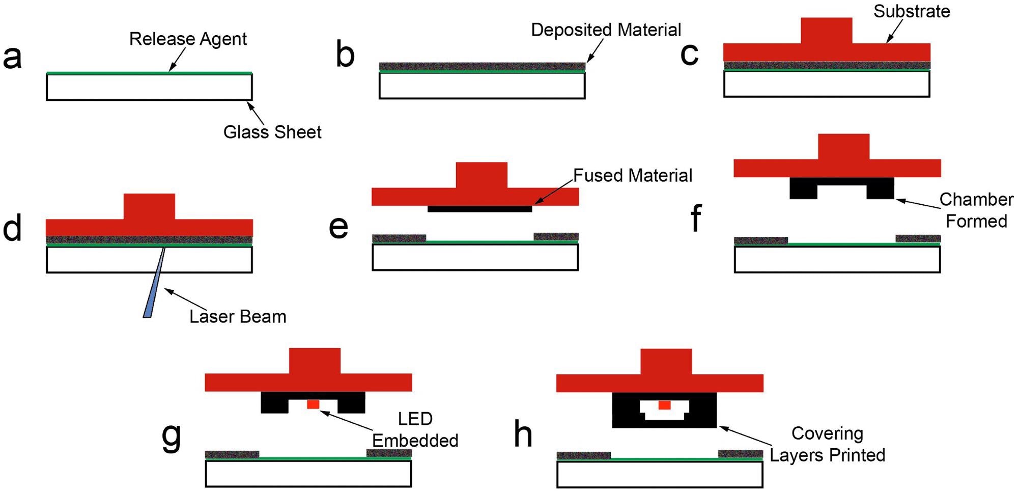
a) The selected release agent is coated onto the glass b) The release agent fluidically captures a single powder material layer c) Substrate is pressed onto the upper surface of the powder d) The laser fuses a selected region of powder to the substrate e) The substrate is raised with the fused powder, the glass is then recoated with a new layer of powder f) The process continues, with several initial base layers and chamber layers being formed g) An LED with wires soldered to it is embedded in the powder chambers, the wires lead out of an open region in the walls of the chamber h) Several capping layers are added to finish embedding the print, there is still a small hole in the side of the chamber regions for the wires to protrude from. Image Credit: Whitehead, J et al., Additive Manufacturing Letters
About the Study
In this study, the authors discussed a method for the embedding of electrical components during the SLS process. An inverted laser sintering (ILS) technology was employed to eliminate the requirement for a powder bed and to produce voids in the printed components with ease.
This technology was demonstrated by the insertion of an LED into an SLS part cavity and then the continuation of the printing process. After multiple layers were placed, the LED was externally activated to validate its functionality. This capability assisted SLS in the transition from the fabrication of passive parts to the fabrication of active systems.
The researchers showed the proposed capability by utilizing the ILS system to fabricate a printed component out of thermoplastic powder with an integrated, functional LED. A set of mirror galvanometers guided the laser, which was controlled by an Arduino UNO microprocessor. A white thermoplastic polyurethane (TPU) powder was employed as the material (Sinterit).
The substrates were made out of an orange acrylic that was opaque to light with a wavelength of 445 nm. The initial printed six base layers acted as a substrate onto which the LED was mounted to create the ILS component. To connect the embedded element to the controlling Arduino, 30 layers of the chamber were added to provide a region having an opening for the leads of LED to channel through.
The team routed the wires out of the aperture once the LED was put to the glue. The LED was adhered to the adhesive for five minutes before being removed. The beam was directed in a nested circular shape for laser sintering.
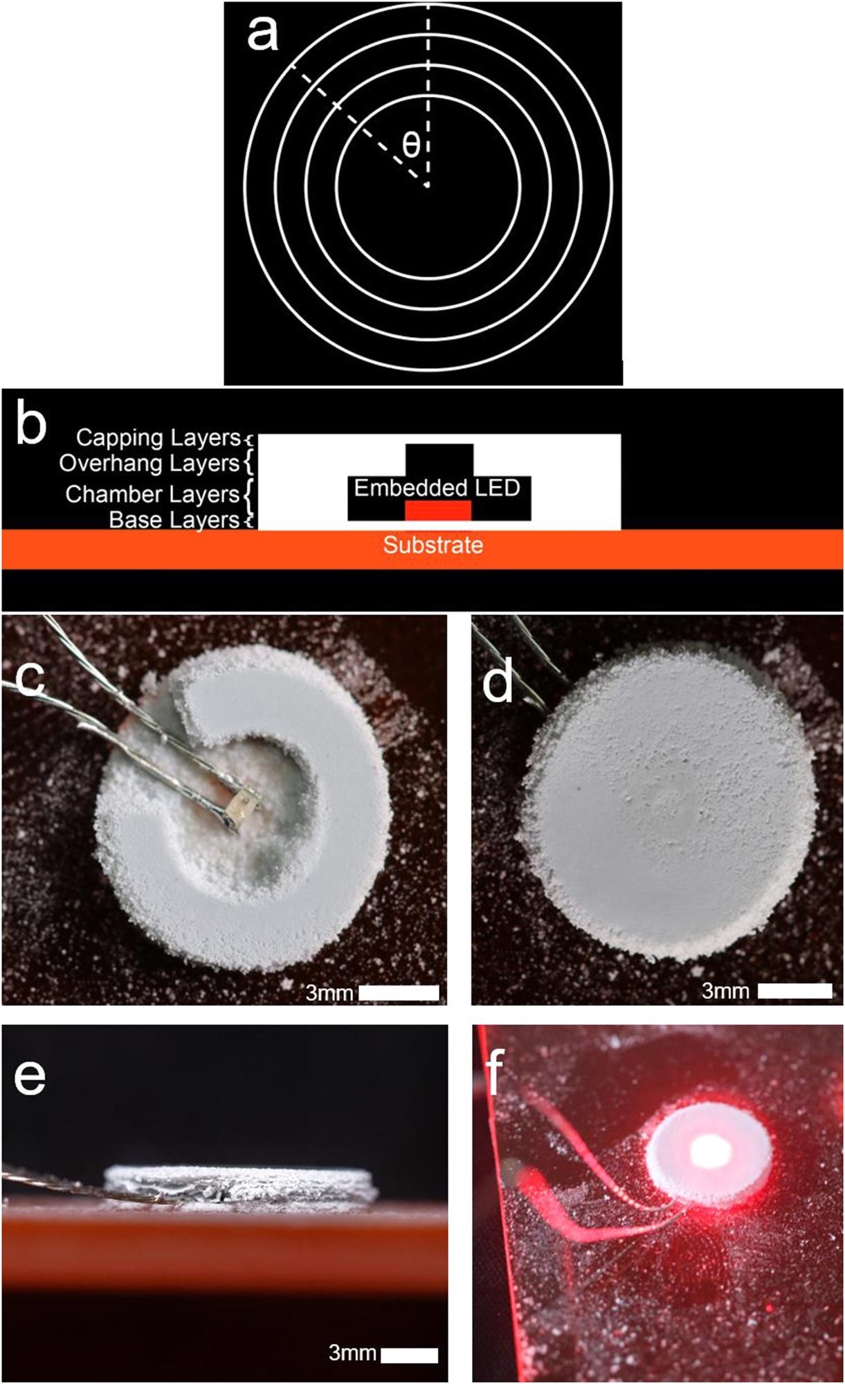
a) Diagram of nested circle layer sintering pattern b) Layer diagram for the embedded LED sample c) Embedded LED adhered to the base layers, surrounded by material in the chamber layers d) Upper surface of the embedded LED sample e) Side view of the embedded LED sample showing the wires f) Activated LED shining through the upper surface of the sample. Image Credit: Whitehead, J et al., Additive Manufacturing Letters
Observations
A 2.06 mm tall, 55-layer TPU component was effectively created with a functional electronic component integrated during printing using SLS printing. This resulted in a layer height of 30 to 40 meters on average. The presence of this light showed that no severe damage to the embedded component (either the cables of the LED) had happened, however some surface damage could have occurred. Any adhesive that covered the LED surface between the laser and the diode during embedding could have averted damage to some extent.
The 3D nature of the printing technique allowed the electronic zones to be stacked and facilitated the formation of functional multi-dimensional electronic circuits. These wires and electronics would not have to be on the same plane or in the same layer region.
Furthermore, because the electronic embedding happened during the printing process and no additional material removal was required without the use of passive support powder, these complicated components would require less post-processing assembly.
Conclusions
In conclusion, this study demonstrated the ILS printing process' ability to create prints with embedded components. The authors emphasized that while the proposed method was used to embed a basic LED with wires which were protruding from the sides, it could also be used to implant more sophisticated components. They believe that in addition to the chambers for electronic components, the print might include pathways where wires could be implanted to connect these embedded elements.
They also mentioned that future work would focus on producing pieces with embedded electronic components which are connected by embedded wires to further illustrate this.
Disclaimer: The views expressed here are those of the author expressed in their private capacity and do not necessarily represent the views of AZoM.com Limited T/A AZoNetwork the owner and operator of this website. This disclaimer forms part of the Terms and conditions of use of this website.