Image Credit: NC State University
Our work here not only means that we can reduce energy loss in power electronics, but we can also make the systems for power conversion more compact compared to conventional silicon and silicon carbide electronics.
Ramón Collazo, Study Co-Author and Associate Professor, Materials Science and Engineering, North Carolina State University
“This makes it possible to incorporate these systems into technologies where they don’t currently fit due to weight or size restrictions, such as in automobiles, ships, airplanes, or technologies distributed throughout a smart grid”, stated Collazo.
In a study released in 2021, the researchers described a method for doping specific regions of GaN materials using ion implantation and activation. To deliberately alter the electrical characteristics of the GaN solely in those places, they introduced impurities into particular sections of GaN materials.
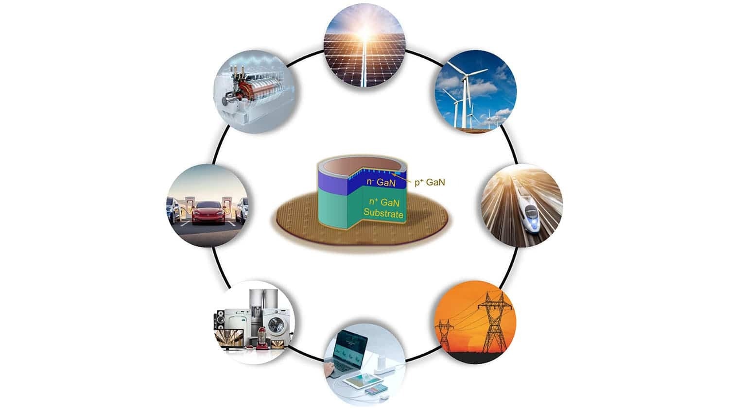
The researchers have shown how this method can be applied to produce genuine devices in their most recent work. To develop Junction Barrier Schottky (JBS) diodes, the researchers specifically employed materials that had been carefully doped with GaN.
Collazo stated, “Power rectifiers, such as JBS diodes, are used as switches in every power system. But historically they have been made of the semiconductors silicon or silicon carbide, because the electrical properties of undoped GaN are not compatible with the architecture of JBS diodes. It just does not work.”
“We have demonstrated that you can selectively dope GaN to create functional JBS diodes, and that these diodes are not only functional, but enable more power efficient conversion than JBS diodes that use conventional semiconductors. For example, in technical terms, our GaN JBS diode, fabricated on a native GaN substrate, has record high breakdown voltage (915 V) and record low on-resistance,” he continued.
Collazo further added, “We are currently working with industry partners to scale up production of selectively doped GaN, and are looking for additional partnerships to work on issues related to more widespread manufacturing and adoption of power devices that make use of this material.”
The study was published in the journal Applied Physics Express.
Spyridon Pavlidis, an assistant professor of electrical and computer engineering at NC State, Shashwat Rathkanthiwar, a postdoctoral researcher at NC State, Hayden Breckenridge, a former PhD student at NC State, Shane Stein, a PhD student at NC State, Erhard Kohn, a research associate at NC State and emeritus professor of Ulm University in Germany, Zlatko Sitar, Kobe Steel Distinguished Professor of Materials Science and Engineering at NC State and the founder of Adroit Materials, Will Mecouch, Seiji Mita, Baxter Moody, Pramod Reddy, James Tweedie and Ronny Kirste of Adroit Materials, and Kacper Sierakowski, Grzegorz Kamler and Michał Boćkowski of the Institute of High-Pressure Physics at the Polish Academy of Sciences are the co-authors of the study.
The majority of the funding for this work came from ARPA-PNDIODES E’s program through grants DE-AR0000873, DE-AR000149. Additional funding for the project came from the National Science Foundation (ECCS-1916800, ECCS-1508854, ECCS-1610992, DMR-1508191, and ECCS-1653383), the Naval International Cooperative Opportunities in Science and Technology program of the Office of Naval Research Global (N62909-17-1-2004), and Poland’s National Center for Research and Development (NCBR) (TECHMATSTRATEG-III/0003/2019-00).
Journal References
Khachariya, D., et al. (2022) Vertical GaN Junction Barrier Schottky Diodes with Near-ideal Performance using Mg Implantation Activated by Ultra-High-Pressure Annealing. Applied Physics Express. doi:10.35848/1882-0786/ac8f81
Breckenridge, M. H., et al. (2021) High Mg activation in implanted GaN by high temperature and ultrahigh pressure annealing. Applied Physics Express. doi:10.1063/5.0038628