By building microscopic copper coils vertically above chip contact pads, researchers tested whether RF inductors can escape the planar space constraints that have long complicated circuit miniaturization.
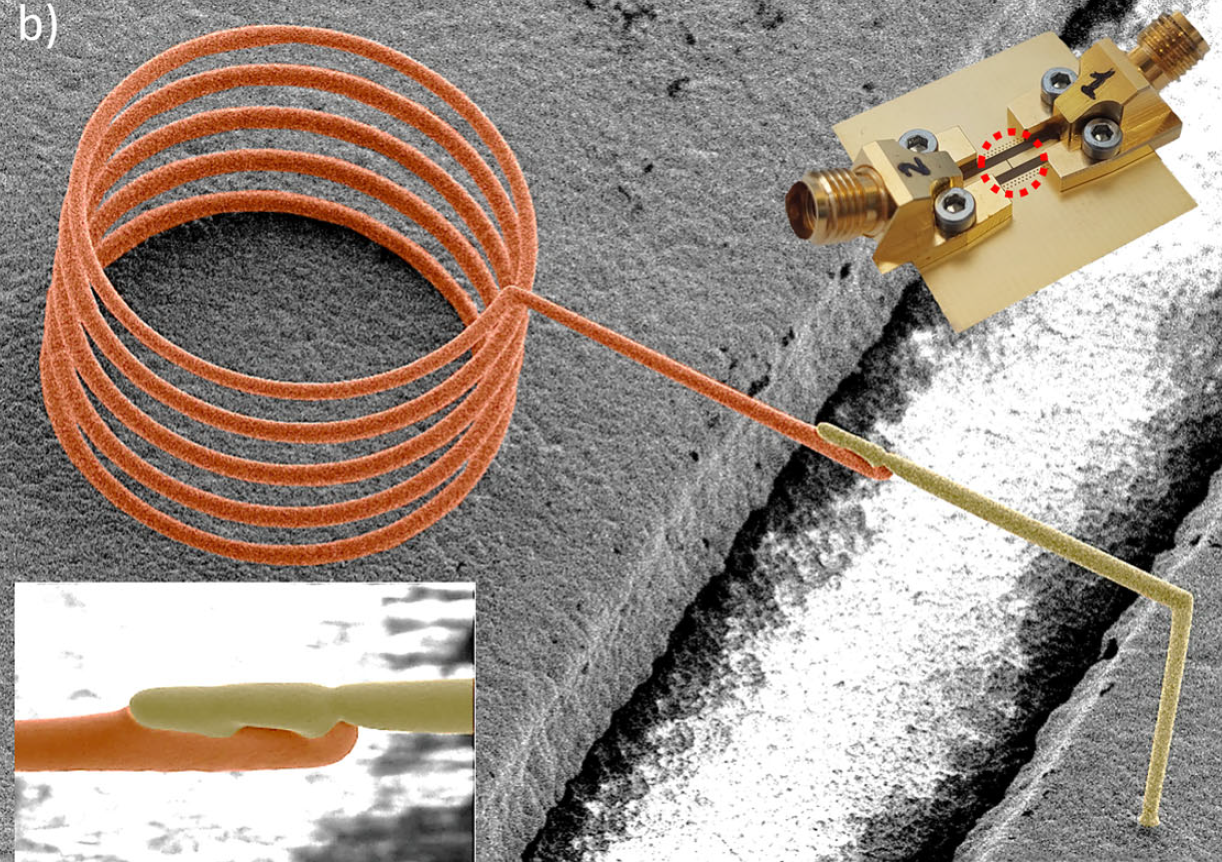
Paper: On-chip 3D printing of metal microinductors for radio frequency electronics
A recent study published in the journal Nature Communications demonstrates a direct metal-printing method for fabricating 3D copper microinductors on chip surfaces.
The researchers used localized electrodeposition to build freestanding copper microsolenoids vertically across contact pads. The printed devices achieved quality factors up to 18 and remained inductive up to 15 GHz.
3D Printing Addresses Space Limitations in Radio Frequency Circuits
On-chip inductors are important components in wireless communication systems, Internet of Things devices, oscillators, mixers, and low-noise amplifiers. However, conventional planar inductors occupy a considerable portion of the silicon die area. Their large footprint can limit circuit miniaturization, restrict layout flexibility, and increase manufacturing costs.
The researchers investigated whether the vertical space above a chip could accommodate inductors without increasing the planar circuit footprint. They directly printed copper microcoils onto the chip contact pads using a room-temperature, maskless electrodeposition process. The resulting structures functioned as freestanding microsolenoids. By extending above the chip surface, they generated inductance without requiring large planar spiral patterns.
In this study, the researchers combined electromagnetic modeling, direct metal fabrication, structural characterization, and radio frequency measurements to examine how coil geometry affected device performance. The results provide a potential route toward compact RF components that could be integrated after standard chip fabrication, potentially improving RF-IC scalability.
Building Freestanding Copper Microsolenoids
The researchers fabricated the microinductors with an Atomic Force Microscopy (AFM) based nanoscale printing system equipped with a 300 nm aperture. A copper ion ink passed through the nozzle and reached selected regions of a conductive substrate. On the conductive substrate, copper ions were electrochemically reduced to form solid copper voxels, which were deposited sequentially to build the three-dimensional structures.
The team selected copper because it offers high electrical conductivity, relatively low cost, and compatibility with established integrated-circuit technologies. The researchers printed the microinductors across a gap in a gold-patterned grounded coplanar waveguide. A vertical copper pillar formed one electrical connection, while a horizontal wire connected the coil to the opposite side of the gap.
The team produced coils with different radii, numbers of turns, coil densities, and wire diameters. Representative devices included five-turn microsolenoids with radii of 20, 40, and 60 μm and wire diameters of approximately 5 μm. The printed structures achieved sub-micrometer dimensional accuracy and an average root-mean-square surface roughness of 41 nm. The printed copper had an extracted resistivity of 19 ± 2 nω ·m, corresponding to about 87% of the bulk copper conductivity. The process also enabled variable-radius coils, series-connected solenoids, and concentric transformer structures. These demonstrations highlight the flexibility of direct metal printing for producing customized three-dimensional RF architectures.
Coil Geometry Determines RF Performance
The researchers used full-wave, three-dimensional electromagnetic simulations to investigate how microinductor geometry affected inductance, quality factor, and self-resonance. The simulations covered frequencies from 1 MHz to 300 GHz and accounted for short coil lengths, fringing fields, and parasitic effects.
Increasing the coil radius increased inductance and quality factor at a given frequency. However, larger coils also generated greater parasitic capacitance, which lowered the self-resonance frequency and narrowed the useful operating range. Increasing the number of turns raised the inductance, but the peak quality factor decreased and shifted to lower frequencies due to increased resistance and parasitic capacitance.
Higher coil density strengthened magnetic coupling between adjacent turns and reduced radiative losses. These effects improved inductance and quality factor, although the accompanying increase in parasitic capacitance again reduced the self-resonance frequency. Experimental measurements agreed with the simulations. The fabricated microinductors exhibited inductance values ranging from approximately 0.8 to 3 nH. At 2 GHz, quality factors ranged from 11 to 16 and increased with coil radius.
Measurements up to 15 GHz showed that the devices maintained predominantly inductive behavior. The inductance remained approximately constant, while the quality factor reached about 18 near 5 GHz. At higher frequencies, the measured quality factor was limited largely by dielectric losses and parasitic effects in the FR4-based test platform rather than by the printed microinductors themselves. Four-probe measurements showed the microinductors’ resistance to be approximately 0.6 to 1.8 Ω, depending on geometry and printing conditions. Sample-to-sample variation in the extracted inductance and resistance remained below 7%, supporting the reproducibility of their electrical performance.
Enabling Compact and Scalable RF Electronics
This study demonstrates that direct metal printing can produce functional copper microinductors on chip surfaces, addressing a major space limitation of conventional planar designs. By extending the coils vertically, the researchers achieved nanohenry-range inductance without requiring additional dedicated planar silicon area.
High-precision electrodeposition and flexible three-dimensional geometries also expand the design options for RF components. The printed microinductors achieved quality factors up to 18 and maintained inductive behavior up to 15 GHz. These results demonstrate their potential for high-frequency operation within the tested measurement platform.
The approach could also support post-fabrication integration. In addition, PDMS encapsulation did not significantly alter the impedance spectra or extracted electrical parameters, suggesting that protective polymer embedding is feasible. However, the study evaluated the microinductors on dedicated test platforms rather than demonstrating them within a complete functional RF integrated circuit. Further studies should examine package-level reliability, thermal management, electromagnetic compatibility, and performance at higher frequencies. Researchers could also improve device performance by increasing copper conductivity, refining coil geometries, incorporating magnetic materials, and testing the structures on dedicated low-loss RF substrates.
Overall, direct 3D metal printing offers a promising route to integrate compact RF inductors and expand circuit design beyond conventional planar architectures. By using vertical space above the chip, this strategy could support smaller, more flexible, and more scalable RF systems.
Disclaimer: The views expressed here are those of the author expressed in their private capacity and do not necessarily represent the views of AZoM.com Limited T/A AZoNetwork the owner and operator of this website. This disclaimer forms part of the Terms and conditions of use of this website.