In 1935, Max Knoll invented the scanning electron microscopy (SEM) in Germany to study the targets of television tubes. Two years later, Manfred von Ardenne built an electron microscope with a highly demagnified probe using two condenser lenses for scanning transmission electron microscopy. He also tried it as an SEM. In 1942, Zworykin and his co-workers at the RCA Laboratories in the USA designed and built a dedicated SEM. In 1948, Sir Charles Oatley and Dennis McMullan built their first SEM at Cambridge University. In 1965, “Stereoscan” — the first commercial instrument — was launched by the Cambridge Scientific Instrument Company for DuPont. (Zhu & Inada, 2016)
How Scanning Electron Microscope Works
The SEM is a microscope that works by scanning a focused beam of electrons on a sample of interest.
The electron beam comes from a filament, which is made of several types of materials. Tungsten hairpin gun is the most common of these materials. This filament is a loop of tungsten which acts as the cathode. A voltage is applied to the loop, causing it to heat up. The anode, which is positive with respect to the filament, forms powerful attractive forces for electrons. This causes electrons to accelerate toward the anode. Lanthanum Hexaboride filaments and field emission guns are other examples of filaments.
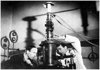
Figure 1. Ruska (right) and Knoll working on their transmission electron microscope (Sciencemag, 2017).
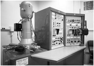
Figure 2. Scanning Electron Microscope at JPL (Cooper, 2017).
SE and BSE Detectors
The SEM produces various types of signals. These include the following: secondary electrons, characteristic x-rays, back scattered electrons (BSE), transmitted electrons and sample current. All these require specialized detectors for their detection that are not usually present on a single machine (Arikan, 2009).
Secondary Electron Imaging
Secondary electron imaging, also called the standard detection mode, is the most commonly used detection mode. The SEM can produce very high resolution images of a sample surface, revealing details about 1 to 5 nm in size in this mode. This is done by collecting low-energy secondary electrons that are ejected from the sample atoms by scattering interactions with beam electrons. (Arikan, 2009).
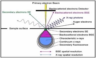
Figure 3. Scanning Electron Microscopy Scheme (Bachmann, 2017).
Beam electrons that are reflected from the sample are referred to as back-scattered electrons (BSE). These are frequently used in analytical SEM, because the intensity of the BSE signal is strongly related to the atomic number of the sample. Images produced by these BSE can provide information about the distribution of different elements in the sample.
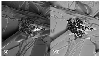
Figure 4. SE and BSE Images (Chung, 2017).
X-Ray Microanalysis Techniques
Depending on the measuring technique applied, two different experimental methods for X-ray microanalysis have been developed:
- Wavelength dispersive X-ray microanalysis (WDX)
- Energy dispersive X-ray microanalysis (EDX)
As the names indicate, in each case the emitted X-ray will be analyzed either as a function of the energy of the emitted radiation (EDX) or its wavelength (WDX).
The EDS x-ray detector measures the relative abundance of emitted x-rays versus their energy. The detector is typically a lithium-drifted silicon, solid-state device. When an incident x-ray strikes the detector, it creates a charge pulse that is proportional to the energy of the X-ray. A charge-sensitive preamplifier converts the charge pulse to a voltage pulse (which remains proportional to the x-ray energy). Then, the signal is sent to a multichannel analyzer where the pulses are sorted by voltage. The energy, as determined from the voltage measurement, for each incident x-ray is sent to a computer for display and further data evaluation. To determine the elemental composition of the sampled volume, the spectrum of X-ray energy versus counts is evaluated. (MEE, 2017)
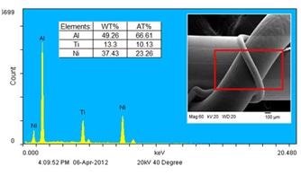
Figure 5. The red rectangle in the inset image shows the selected EDX inspection field. The resulting spectrum and tabulated results reveal that Al, Ti, and Ni are the main elements present with Al being the most abundant in the selected field. (Anderson, 2017).
Tabletop Scanning Electron Microscopy: Making SEM Technology Easier and Reachable
SEM Technology is a crucial solution for numerous fields of research; but usually it is costly and inaccessible. Specially trained operators are required for the operation of a traditional scanning electron microscope, and it is generally not easy.
As a solution to all these issues, table top scanning electron microscopes provide a profound resolution. At this point SEMOSCOPE of Inovenso plays an important role.
Inovenso’s R&D department — with nine years experience in the field of nanotechnology and extensive research — came up with a Benchtop Scanning Electron Microscope that is the size of an old computer. This device can be installed very easily, requires minimal maintenance and is able to speed up the research in the field of nanotechnology. It enables researchers to take high-quality images at a very high magnification in less than five minutes.
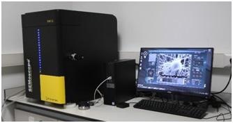
Figure 6. Semoscope.
The following are the four models of Compact Scanning Electron Microscopes that Inovenso has launched:
IEM 10: A benchtop SEM with BE detector and a magnification up to x100,000.
IEM 11: A benchtop SEM with BE and BSE detectors and a magnification up to x150,000.
IEM 10+: A benchtop SEM with BE and EDS (X-ray) detectors and a magnification up to x100,000.
IEM 11+: A benchtop SEM with BE, BSE and EDS (X-ray) detectors and a magnification up to x150,000.
The following are the advantages of SEMOSCOPE
- Minimal preparation actions of the sample
- Simple and quick installation
- No maintenance needed
- No special operator training needed
- Three times more affordable than a conventional SEM
- Obtains results in less than four minutes
- Magnification ranges between x20 and ~ x150,000
- Resolution is 5 nm
- Easy navigation with user-friendly software
- No infrastructure required
- Efficient after-sales service
IEM10: Benchtop Scanning Electron Microscope
SEMoscope IEM10 Benchtop SEM is a portable scanning electron microscope and is ideal to observe the depth with a magnification up to x100,000. It has the features of an SE detector, which enables the user to shoot high-quality images in less than four minutes.
Specifications
- Magnification up to x 100,000
- Auto Stage: X, Y, T Axis
- Click & Move Stage Control
- Auto Function: Filament Memory, Focus, Contrast, Brightness
- High Definition Image : 5120 X 3840 Pixel
IEM10+: Benchtop Scanning Electron Microscope
SEMoscope IEM 10+ Benchtop SEM, an advanced version of the model IEM10 scanning electron microscope, has SE and EDS detectors. It is a useful analytical tool in many fields, from materials science and nanotechnology to biology and microelectronics.
Specifications
- Magnification up to x 100,000
- Auto Stage: X, Y, T Axis
- Click & Move Stage Control
- Auto function: Filament Memory, Focus, Contrast, Brightness
- High-definition image: 5120 X 3840 Pixel
- Thermo EDS detector: 133 eV at Mn, B(5) ~ U(92)
IEM11: Benchtop Scanning Electron Microscope
SEMoscope IEM 11 Desktop SEM is the world’s fastest desktop scanning electron microscope. This device is an ideal substitute for traditional SEMs with its high magnification up to x 150,000. It has SE and BSE detectors, which will enable users to conduct analyzes up to a nanoscale in a very short span of time.
Specifications
- High quality images (5 nm resolution)
- Magnification up to x 150,000
- Easy navigation with the “Navigation Mode”
- Precise control with a joystick and the “Driving Mode”
- Combined SE and BSE images
- Low energy consumption
- Intuitive user interface
IEM11+: Benchtop Scanning Electron Microscope
This is the world’s most advanced desktop scanning electron microscope. This device does not rely on a single detector and combines three different micro-analytical detectors: SE, BSE and EDS. By using EDS to complement other detectors, users can take advantage of the specific advantages of EDS, in terms of speed and relative ease of sample preparation, to acquire a full elemental spectrum in just a few seconds.
Specifications
- High-quality images (5 nm resolution)
- Magnification up to x 150,000
- Easy navigation with the “Navigation Mode”
- Precise control with a joystick and the “Driving Mode”
- Combined SE and BSE images
- Low energy consumption
- Intuitive user interface
- Oxford:130 eV at Mnk, C(6) ~ U(92) / EDAX:133 eV at Mnk, Be(4) ~ U(92)
References
- (2017, 11 07). Retrieved from Sciencemag: http://poster.sciencemag.org/sem/#intro
- Anderson. (2017, 11 08). Anderson Materials. Retrieved from Anderson Materials: https://andersonmaterials.com/energy-dispersive-x-ray-microanalysis-edx-eds-in-depth/
- Arikan, S. (2009). Improving Quality of Electron Microscopic. Delft: Delft University of Technology.
- Bachmann, K. (2017, 11 08). Helmholtz-Zentrum Dresden-Rossendorf. Retrieved from Helmholtz-Zentrum Dresden-Rossendorf: https://www.hzdr.de/db/Cms?pOid=65929&pNid=0
- Chung, P. (2017, 11 08). University Of Glascow ISAAC : Imaging Spectroscopy and Analysis Centre. Retrieved from University Of Glascow ISAAC
- Cooper, J. (2017, 11 07). About Us: The Jet Propulsion Laboratory-NASA. Retrieved from TJPL-NASA: https://www.jpl.nasa.gov/blog/2012/5/scanning-electron-microscope
- David C. Joy, B. J. (2017, 11 07). Encyclopædia Britannica.
- Herres, D. (2017, 11 07). Test and Instrument Tips.
- MEE. (2017, 11 08). Materials Evaluation and Engineering, In.
- Michler, G. H. (2008). Electron Microscopy Of Polymer. Verlag Berlin Heidelberg: Springer.
- Postek, M. (2016). Comparison of Electron Imaging Modes for Dimensional Measurements in the Scanning Electron Microscope. Microscopy and Microanalysis, 768-777.
- Wells, O. C., & Joy, D. C. (2006). The early history and future of the SEM. Surface and Interface Analysis, 1738-1742.
- Zhu, Y., & Inada, H. (2016). Encyclopedia of Nanotechnology. Springer Netherlands.

This information has been sourced, reviewed and adapted from materials provided by Inovenso SEM.
For more information on this source, please visit Inovenso SEM.