Conventional energy dispersive X-ray spectroscopy has been run at high X-ray energies as this gives less background noise and improved line separation. However, modern analysis in semiconductor-based technologies or advanced alloys, needs an improved spatial resolution.
Ultim® Range of EDS Detectors
To provide optimum sensitivity when working under these difficult conditions the Ultim® range of EDS detectors uses optimized geometries in combination with the largest area SDD to reliably provide an improved count rate.
To be able to analyze samples with finely detailed structures, such as the NAND Flash memory device in this article which has features of sizes between 10 – 500 nm, a high spatial resolution is required.
Analyzing NAND Flash Memory Device Through Low kV EDS
The NAND Flash sample also contains a range of different elements that cover a broad portion of the X-ray spectrum. To achieve a high EDS resolution the volume from which X-rays are generated must be reduced. The X-ray generation volume for L-series X-rays in pure iron, and the volume reduction as the energy of incident electrons is reduced from 20 kV to 1 kV is shown in Figure 1.
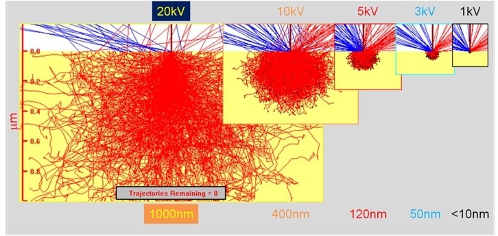
Figure 1. Monte Carlo simulations of the generation volume of Fe Lα X-rays in pure Fe at varying electron energy.
Reducing the energy of incident electrons also means that less X-rays are produced and there are fewer available X-ray lines. For example, varying the incident electron energy from 20 kV to 10 kV for pure iron under the same conditions results in a 90% reduction in K-series X-ray lines (a significant reduction) and no change in the L-series. Reducing the energy to 5 kV or 3 kV results in a 100% reduction in K-series line and respective 50% or 80% reductions in the L-series.
To overcome this loss in counts the sensitivity of an X-ray detector must be maximized. The sensitivity of a detector is defined by the solid angle that it subtends. Generated X-rays are emitted in a hemisphere from the surface of the specimen at the incident beam position. The solid angle of a detector is the amount of this hemisphere that it captures and can be described by dividing the area of the detector (A) by the distance between the detector and the sample squared (d2).
solid angle ~ A ⁄ d2 (1)
The solid angle can be increased, and therefore the number of counts collected, by maximizing A and minimizing d. When working at very low electron energies, which give very low count rates, the detector should be as close to the sample as possible as this will give the best sensitivity (Figure 2).
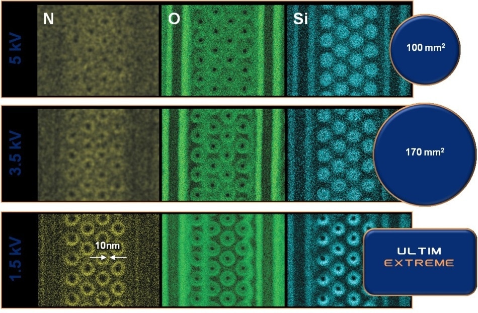
Figure 2. EDS maps for N, O, and Si collected from a NAND flash memory device with Ultim Max detectors of 100 mm2 and 170 mm2 sensor areas and Ultim Extreme.
In order to improve the spatial resolution the current of the incident beam must also be minimized due to the Boersch effect. To account for this the experiment was run with an incident electron beam current of approximately 160 pA. This gave an input count rate of 1,600 cps for the Ultim Max 100 at 5 kV and a sample-detector distance of 7 mm. At these conditions EDS data was gathered for an hour.
At an energy of 5 kV the EDS maps can be used to differentiate between key structures in the sample such as the oxide and silicon areas, and tungsten word lines (these maps are not shown). The oxygen map shows faint structures surrounding “holes” in the map, and faint structures can also be seen in the nitrogen map.
Reducing the electron energy to 3.5 kV means that even more structure becomes visible. In the oxygen map it becomes obvious that there are separated rings surrounding the “holes” in the 5 kV map. These rings correspond to rings seen in the silicon map, and the presence of ring-structures in the nitrogen map indicates each of these rings has a complex layered structure.
Factor for Improving Spatial Resolution in Elemental Mapping
This demonstrates that low energy is the most important factor in improving the spatial resolution in elemental mapping. Improving instrument sensitivity towards X-rays of very low energies is possible by removing the X-ray window, which often absorbs 100% of sub kV X-rays. Ultim Extreme has a windowless design made to work at extremely short analytical distances to optimize sensitivity at enhanced spatial resolutions.
Using the same conditions as above but with the Ultim Extreme at a 4.5 mm working distance and 1.5 kV energy the count rate was 5,200 cps. This enhanced count rate meant scanning the sample took only 30 minutes. At 1.5 kV even more details where visible in the EDS maps, such as clearly defined nitrogen rings within the device’s charge traps. Highly specific surface features can also be observed in the oxygen maps, such as artifacts from variations in ion milling that occurred during sample preparation.
At the very low energy of 1.5 kV the X-ray lines usually used for silicon or tungsten cannot be used. Instead lower energy lines such as LI (0.092 keV) for silicon and N5N6 (0.210 keV) for tungsten can be used. The windowless design of the Ultim Extreme means that these lines can be collected at efficiencies above 80% meaning that accurate elemental maps can still be constructed (Figure 3).
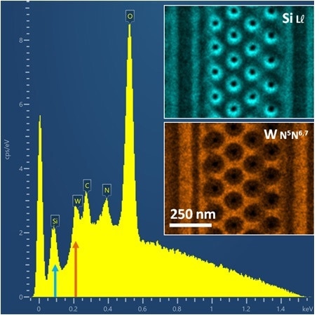
Figure 3. 1.5 kV EDS spectrum showing low energy X-ray lines of Si Ll (0.092 keV) and W N5N6, 7 (0.210 keV). Inserts show elemental mapping using these two X-ray lines.
Equally important to data acquisition is data processing. AZtec TruMap can be used to remove any background radiation and deconvolute peak overlaps in real time. This allows accurate elemental maps to be drawn which are free from spectral artifacts (Figure 4).
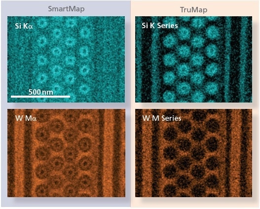
Figure 4. Si and W maps collected at 3.5 kV processed using window integral mapping and AZtec TruMap.
At electron energies between 2.5 kV and 5 kV silicon and tungsten can be analyzed using their K and M lines, which are 1.74 keV and 1.77 keV respectively and these lines show strong overlap. This overlap means that when mapping Si K with a window integral (SmartMap) both silicon and tungsten structures are observed.
TruMap can be used to solve this problem as it can display only real silicon counts, and therefore the true silicon distribution in the sample.
Conclusion
Improving the sensitivity of an X-ray detector by reducing the sensor-sample distance and/or sensor size, or by removing the window, makes it possible to collect low-energy X-rays at high counts; allowing elemental maps to be collected at resolutions of less than 20 nm, even for light elements.

This information has been sourced, reviewed and adapted from materials provided by Oxford Instruments NanoAnalysis.
For more information on this source, please visit Oxford Instruments NanoAnalysis.