The latest research in ACS Applied Energy Materials has shown that vertically aligned silicon nanowire (VA-SiNW) arrays are capable of massively increasing light absorption and causing a significant reduction in light reflection.
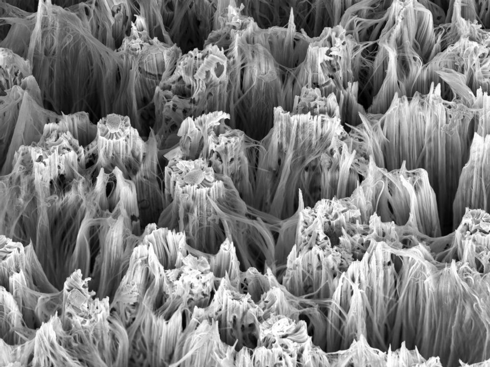
Silicon nanowires observed with an electron microscope. Study: Recent Advances in Structuring and Patterning Silicon Nanowire Arrays for Engineering Light Absorption in Three Dimensions. Image Credit: Roberto Lo Savio/Shutterstock.com
The study deduces that such structures can boost the design of solar cells via the synthesis of thin and efficient silicon-based solar cells. Controlled structure and patterning of Si in three dimensions can give an extra degree of flexibility by allowing for three-dimensional control of light absorption.
Optoelectronic Properties of Si – Nanowires
A variety of optical effects such as waveguiding, diffraction effects, moth-eye effect, Fabry-Perot resonances, and near field coupling are observed due to light interaction.
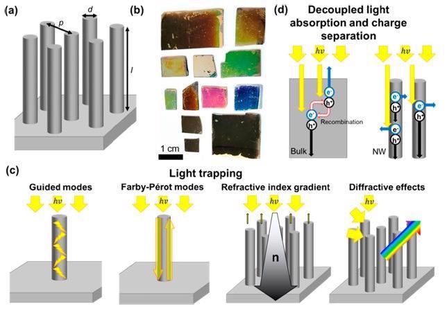
Optoelectronic properties of SiNW arrays. (a) Scheme showing the geometrical parameters that can be easily adjusted during the synthesis of SiNW arrays: wire diameter (d), length (l), and array pitch (p). (b) Photographs of various SiNW arrays synthesized in our laboratories showing colors that cover the whole visible spectrum, including black silicon surfaces that significantly trap the incident light. (c, d) Schematic illustration of (c) various light trapping effects that can lead to enhanced absorption, reduced reflection, and diffraction; and (d) decoupled light absorption from the charge separation process that can lead to reduced charge recombination. Image Credit: Bartschmid, T et al., ACS Applied Energy Materials
Leaky Waveguide Effect
Silicon nanowires can operate as subwavelength dielectric tubular waveguides, guiding and trapping light within the wire and resulting in increased light absorption at certain wavelengths. The diameter-dependent waveguiding behavior of SiNWs with diameters in the range from 25 to 300 nm was investigated by Leu et al.
Fabry-Perot Resonance
Fabry-Perot resonances may be sustained in VA-SiNWs irradiated at normal incidence (i.e., parallel to the NW long-axis), where the incoming light is reflected at the bottom and top of the nanowire array to generate a standing wave, resulting in a distinctive dip in the reflectance spectrum. When the round-trip nanowire length 2l = m eff, where m is an integer, such Fabry-Perot cavities are seen.
Moth Eye Effect
Pristine silicon solar cells reflect a significant percentage of incident solar light (i.e. >30 percent in the UV to near-IR spectrum) because of the high refractive index of silicon. This is because light reflection occurs and is greatest when two surfaces have a sudden and substantial shift in refractive index.
Because of the so-called moth-eye effect, nanostructured interfaces such as silicon nanowire arrays can progressively modify the refractive index, resulting in a considerable drop in substrate reflectivity.
Diffractive Effects
Diffractive effects may be seen in periodic arrays of nanowires. Vivid structural colors may be seen depending on the diffraction order, wavelength, incidence angle, and array pitch.
Decoupled Light Absorption
SiNWs profit from their one-dimensional shape, which can isolate light absorption from the charge separation process, in addition to their better optical qualities compared to bulk silicon. The recombination of photoexcited electric charge before extraction can lower conversion efficiency in a photovoltaic or photocatalytic system.
Classical Methods
The independent control of nanowire form, size, and composition is a fundamental problem in the synthesis of SiNW arrays. By selectively altering dopant concentrations, vapor-liquid-solid (VLS) syntheses may be changed to provide fine control over nanowire diameter in the axial direction during the VLS development, throughout the lengths of the nanowire, in conjunction with selective chemical etching or by adjusting the catalyst droplet size.
Metal Assisted Chemical Etching (MACE) and Colloidal Lithography
During MACE, a Si wafer is submerged in a solution coated by a nanostructured metal, generally consisting of a noble metal such as Au, which generally contains hydrofluoric acid (HF) and an oxidant peroxide (H2O2). In the presence of HF, the holes are transmitted through the metal and injected into the silicon, which oxidizes and dissolves, producing hydrogen gas as a byproduct.
The use of colloidal lithography and MACE to synthesis VA-SiNW arrays with programmable geometries is a tabletop, cost-effective, and adaptable method.
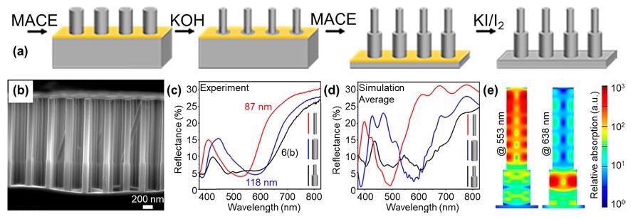
Bisegmented VA-SiNW arrays. (a) Schematic representation of the synthesis route using sequential MACE and KOH etching steps. (b) Secondary electron SEM image of bisegmented VA-SiNWs with top and bottom diameters of dbi,top = 98 nm and dbi,bottom = 133 nm, respectively. (c) Measured reflectance spectra of two different VA-SiNWs with a single-diameter of dsingle1 = 87 nm (red curve) and dsingle2 = 118 nm (blue curve). The black curve shows the measured reflectance of the bisegmented structure shown in panel b. (d) Simulated reflectance spectra corresponding to the VA-SiNWs shown in panel c, same color code. (e) Two-dimensional maps of the simulated relative absorption within one SiNW in the bisegmented VA-SiNW array simulated at 553 and 638 nm, with similar dimensions to the wires shown in panel b. Adapted from ref 11. Copyright 2020 American Chemical Society. Image Credit: Bartschmid, T et al., ACS Applied Energy Materials
Low-Resolution Patterning
Additional materials may be deposited on silicon nanowire arrays using a variety of processes. Electrochemistry is the most promising method for patterning particular portions of SiNW arrays. Conformal metal shells can be electrodeposited on the top of the wires by masking the bottom of the array with a photoresist layer.
Structuring and Patterning for Light Absorption
A mixture of colloidal lithography and metal-assisted chemical etching is used to create the SiNW arrays (MACE).
Exotic SiNW morphologies with elliptical or hexagonal cross-sections, segmented nanowires by combining MACE and KOH etching, substrates with graded optical properties using a dip-etching technique, and Si nanowires functionalized with plasmonic or catalytic nanostructures located at well-defined locations along the nanowires using three-dimensional electrochemical lithography are all possible with the benchtop approaches (3DEAL).
Modification of the original 3DEAL was done to arrange SiNW arrays with insulating SiO2 shells, which guide the electrochemical deposition specifically at the exposed areas on the SiNW surface, providing the community with a synthetic platform that allows for such sophisticated research.
To summarize, the top-notch properties of VA-SiNW arrays make them the best candidate for solar cells. The structuring and patterning optimized the silicon nanowire enhancing light absorption characteristics, making them viable for other research purposes.
It is safe to say that the synthetic method should benefit most organizations interested in and working on nanostructured silicon substrates, since it uses basic benchtop and chemical procedures that are accessible to most researchers.
References
Bartschmid, T., Wendisch, F. J., Farhadi, A., & Bourret, G. R. (2021). Recent Advances in Structuring and Patterning Silicon Nanowire Arrays for Engineering Light Absorption in Three Dimensions. ACS Applied Energy Material. https://pubs.acs.org/doi/abs/10.1021/acsaem.1c02683
Disclaimer: The views expressed here are those of the author expressed in their private capacity and do not necessarily represent the views of AZoM.com Limited T/A AZoNetwork the owner and operator of this website. This disclaimer forms part of the Terms and conditions of use of this website.