The current media environment is rich with opinion. Thus, offering contextual background for the data behind opinions can be just as, if not more so, important than providing the opinion itself. Focusing on the wider context, not just on data coming from the narrow field of interest, is therefore crucial to avoid incorrect assumptions.
This approach is particularly important in microscopy, where it can be tempting for scientists and engineers to focus on the smallest of details in their material investigations, potentially resulting in incomplete conclusions.
For instance, imagine the cross-section prepared by FIB is not large enough and made at a location without defects. Would the conclusion be that the material produced is flawless? What if 3D tomography is performed on a limited volume and shallow depth, unearthing small grains overall? Would this be the basis for a definitive validation of the sample structure hypotheses, even though the situation may be varied across the breadth of the area of interest?
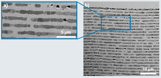
Figure 1. FIB-SEM cut through the layers of an MLCC electronic device. a) This high magnification view of a 10x20 μm area from the polished cross section appears to show a surface with minimal defects in the material. b) By viewing at a lower magnification, we now see numerous defects and their distribution. Image Credit: Tescan USA Inc.
Acquiring information from various viewpoints and scales provides the contextual information required to form valid conclusions that lead to improved research outcomes or optimized future products. This premise is demonstrated in Figure 1, which illustrates two images of the same polished cross-section. Analyzing these images independently, it could be concluded that the sample in Figure 1a has minimal defects on the surface, whereas Figure 1b demonstrates a larger number of defects.
Viewing the same cross-section at lower magnification demonstrates the necessity of a multiscale method in the analysis of material defects. If only the smaller cross-section area is studied, it may be incorrectly assumed that the overall quality of the MLCC microelectronic device is good. A greater field of view reveals the reality of the sample’s defects and their distribution, which results in an entirely different conclusion about the quality of the material.
In the multiscale approach, Scanning Electron Microscopy (SEM) can be used to investigate features well below <50 nm, recording their size, material contrast, topography, or composition. Their location on the sample (often in a mm-size area) can also be documented, as well as their overall distribution and heterogeneity across the sample surface.
This applies equally to Focused Ion Beam–Scanning Electron Microscopes (FIB-SEM) where, in addition to surface characterization, the multiscale approach can be applied to sub-surface applications including cross-sectioning or 3D FIB-SEM tomography.
Obtaining Valuable Surface Contrast Information While Taking Advantage of the Multiscale Approach
Electron microscopy is predominantly used to investigate samples at the nanoscale, allowing for the characterization of the most minute details at high magnification. This helps in understanding the structure of a material and its implications for physical and mechanical properties, as well as the over-arching quality of the materials.
However, the acquisition of data using only a narrow field of view and at high magnification can result in misleading conclusions. The contextual information, acquired at the macro-scale, also helps in determining the whole picture. The broader field of view provides information about the location of the specific feature of focus, offering access to more reliable statistical information about the material.
Figure 2 demonstrates how different levels of magnification reveal critical information about the tungsten carbide magnetic powder sample. The image with the highest magnification (Figure 2a) offers a detailed look at the sample surface and reveals tiny particles of a few nanometers in size.
By viewing the sample from a wider field of view (Figure 2b), it becomes clear that the particles differ greatly in their shapes and sizes, and that they are non-uniformly distributed. By zooming out to a micron-scale view (Figure 2c), it is clear that nanoparticles are part of a large, globular cluster.
Considering that these particles are used as precursor material, all the aforementioned data is needed to predict the characteristics of the final materials and allow for appropriate adjustments to the production process. This clearly shows the importance of acquiring data at multiple scales.
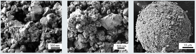
Figure 2. SEM image of magnetic tungsten carbide sample acquired at different magnifications, imaged at 2 keV accelerating SEM voltage. Image Credit: Tescan USA Inc.
Obtaining a single image at high magnification may result in the incomplete characterization of a specimen, and potentially lead to the wrong conclusion. It should also be considered that these characterizations are made using a range of contrast methods, so the ability to distinguish contrast based on energy and angle results in additional information.
Expanding acquisition to be inclusive of dedicated analytical detectors ushers in a new level of comprehension and adds the multimodality that is often leveraged for the evaluation of materials. Each of these analytical and contrast methods adds to this multiscale approach and they are made possible using a SEM column with ultra-high resolution (UHR) capability.
Extend the Characterization Potential From 2D to 3D Using FIB-SEM
FIB-SEM is engineered to perform site-specific cross-sectioning, sample fabrication, and sample modification with an ion beam, either gallium FIB or Xe plasma FIB. This expands characterization to underneath the sample surface. Using FIB to incisively remove material provides access to the sample’s Z dimension, leading to more comprehensive data from the sample. This data can typically be obtained from a single cross-section, 3D FIB-SEM tomography reconstructions, prefabricated micro-testing specimens, or TEM/STEM samples.
3D and cross-sectional tomography and data frequently contain both detailed and multiscale information. To understand a feature or other details in context, the target area must be representative of the studied feature. It needs to contain enough statistical data to be relevant for determining overall material characteristics.
Typically, the boundaries of a cross-section or 3D tomography are defined based on the features of interest in the sample. This varies between samples. For example, for a metal sample that contains conventionally sized grains around the micrometers to ten micrometers, the required volume for investigation could be as high as 500x500x500 μm3.
Smaller grains, those ranging in the sub micrometers size, will need a smaller analyzed volume. A larger area will bring the benefit of improved statistics or a clearer image of a material’s crystallography or phase distribution. Features of interest can also occur deep in the sample and a wide cross-section within sufficient depth will not result in relevant information.
Figure 3. MLCC electronic component analyzed through the metal/ceramic layers embedded in the device. Image Credit: Tescan USA Inc.
Characterization of Features Located Deep Within the Sample’s Structure
A large-scale feature of interest, or a feature buried deep inside a material, nearly always dictates the demand for a deep and large cross-section. For example, structured materials or composites that contain thick coating or multiple layers. These samples require the removal of large amounts to access and visualize any localized defects and other details within the context of the surrounding material. Figure 3 shows an example of this.
MLCC microelectronic components are comprised of multiple ceramic and metallic layers with a total thickness of 300 μm. This system of layers is entrenched deep within a structure. A large area was removed to create a cross-section with enough size to visualize the layer stacks and seek defects within the structure. Here, a cross-section was prepared that is 500 μm wide and more than 300 μm deep.
Even with the ability to analyze detailed information that occurs deeper in the material, a large area had to be unearthed first to acquire enough statistical data about the sample and reveal the defect’s spread over a large area. This process is also required for multilayer materials, coatings, and for many alloys.
For these materials and others similar, it is important to capture all interfaces and characteristics in a statistically representative volume to evaluate adhesions and defects. A multiscale approach is needed here, as both the distribution of features and their location related to the surrounding material offer crucial data for arriving at correct conclusions.
Capture Meaningful and Sometimes Unexpected Results When Analyzing Large Volumes Using Detailed 3D FIB-SEM at the Millimeter Scale
A statistically meaningful representation of the results is a critical parameter when it comes to qualified decision-making in materials science. The same can be said for FIB-SEM analysis of materials, where the features and structure dictate how large the analyzed volume needs to be for materials evaluation.
The area for analysis can be determined using a few parameters. When a repetitive structure within the sample is the area of interest, the minimum analyzed volume can be determined based on the number of features needed to ensure an accurate representation of all structures in the sample. This is not typically challenging for nanoscale features because, in this case, a volume of several μm3 may be enough.
However, in the case of microscale features, a small volume might not represent the whole sample being analyzed. Small volumes are good for providing valuable data mostly on homogeneous samples with small features.
It is a completely different situation in cases where features are different throughout a large sample’s surface, as well as in cases where there is a need to analyze large features of interest.
Figure 4 illustrates the analysis of the shell structure of Argonauta hians. The shell’s structure was characterized by utilizing the contrast around the grain boundaries. The grain size distribution showed substantial variance across the sample volume, but the anticipated average grain size was approximately 500 nm in diameter. To confirm the grain size, material contrast was used to identify the nanometer-thick grain boundary.
 Smaller reconstructed volume 26x25x29 µm3 b) Larger volume 49x 32x32 µm3. (The Argonauta hians specimen is courtesy of Prof. Antonio Checa, University of Granada, Spain.).")
Figure 4. 3D FIB-SEM tomography reconstruction of the Argonata hians shell sample. a) Smaller reconstructed volume 26x25x29 μm3 b) Larger volume 49x 32x32 μm3. (The Argonauta hians specimen is courtesy of Prof. Antonio Checa, University of Granada, Spain.)
To meet the requirements for a high level of detail within a large volume, analyses were conducted at a larger field of view (shown in Figure 4). 3D FIB-SEM tomography offers greater data for analysis, which, in this case, resulted in the correct scientific conclusions about the grain sizes.
Examining the large volume showed more parameters previously unknown: the dominant orientation of the grains. This would have been impossible if a small volume had been analyzed. Determining the grain orientation in both shape and space provides a deeper understanding of the material characteristics and the process of grain growth.
Obtain Meaningful And Representative 3D Analytical Results in the Context of the Complete Sample Volume
Materials are made to match the physical or mechanical properties needed for their ultimate function. In the example of cutting tools, the coating material is made to be durable to ensure that it can cut through hard materials without damaging the tool’s sharp edge. That same cutting tool might also require enhanced material toughness in the central part of the tool.
It can then be presumed that material phases, material chemistry, and grain size distribution will be adjusted according to their position in the tool. Investigating larger areas from the sample helps in understanding the change of the properties that are pertinent to the functionality of the entire device, tool, or component.
Analyzing larger areas is significant in cases where the properties gradually change. A slow change in material properties may arise during the preparation of material due to heat or chemical treatment, or the use of external force to form the material. The evaluation of large areas provides greater precision compared to the extrapolation of results from smaller measurements.
 3D EBSD FIB-SEM tomography of cold drawn wire. b) 3D grain size distribution.c) Grain size on position. d) Grain shape analyses. e-f) 3D grain reconstruction.")
Figure 5. a) 3D EBSD FIB-SEM tomography of cold drawn wire. b) 3D grain size distribution.c) Grain size on position. d) Grain shape analyses. e-f) 3D grain reconstruction. Image Credit: Tescan USA Inc.
Figure 5 demonstrates the 3D EBSD analyses of cold-drawn copper wire. The EBSD analysis facilitates the precise definition of the material phase distribution, similar to that of grain size distribution. 3D FIB-SEM tomography provides the dimensional context lacking in 2D data. This context is important for studying and gaining comprehension of grain shape or orientation in the material.
Viewing the entire volume facilitates the precise evaluation of data relevant to their position in the sample. In this sample, the preparation of only small datasets would have resulted in information that is only relevant to the outer part of the wire, just a few μm below the wire surface. To analyze and visualize the inner structure, the wire can be cut using FIB.
3D EBSD FIB-SEM tomography enables the reconstruction of not only the entire volume but the single grains as well. Not only is the grain size distribution varied, but there are also two different grain shapes. Using this contextual information, it is possible to predict the mechanical properties of the material as an extrapolation for the whole volume.
The relative positions of each grain size or their distribution provide a method of predicting the material properties for the whole material volume from a statistical point of view. In the example of cold-drawn copper wire, it can be confirmed that the material preparation process resulted in the creation of the grain shape distribution and size that 3D EBSD data show.
How Electron Microscopy Supports Multiscale and Multimodal Material Characterization
Collecting data from a multitude of scales, with enough contextual information, is an important step to ensuring valid conclusions that lead to improved research outcomes or optimized future products. Using SEM to understand feature size, material contrast, topography, or composition is important.
However, it is also important to know a feature’s location within the sample as well as its general distribution and heterogeneity throughout the sample surface to make accurate conclusions about the material being evaluated. The multiscale approach of FIB-SEM can be applied to sub-surface applications, including cross-sectioning or 3D FIB-SEM tomography.
Some fields of application—for example, the research of metals, hard coatings, ceramics, and other materials science studies—necessitate supreme analytical characterization capability, while other fields—like semiconductors—require ultimate resolution for imaging and failure analysis.
Theoretically, improvements that address one application field might put a limitation on the performance in other application fields; however, TESCAN FIB-SEM instruments can address this multimodal, multiscale difficulty in materials science, while also maintaining maximum flexibility and superior SEM resolution.
TESCAN’s unique Ultra High Resolution Brightbeam™ column featured on TESCAN’s AMBER FIB-SEM and TESCAN AMBER X plasma FIB-SEM enables the observation of any sample, including materials with magnetic properties, while also allowing multiscale characterization of the sample through the Wide Field Optics™ design.
This expands superior UHR imaging capability to large field-of-view imaging and improves analytical technique capabilities by maintaining high resolution while high analytical currents are in use. Wide Field Optics is particularly valuable for navigation and large-area analyses.
TESCAN BrightBeam™ SEM column is equipped with a rich set of in-column and chamber electron detectors that can acquire up to eight signals at the same time to obtain beneficial sample contrast information. As an analytical column, it is designed to reach up to 400 nA current, which accelerates the acquisition of EDS and EBSD data.
On the FIB side, Ga FIB-SEM and Xe plasma FIB-SEM each support multiscale investigations. The maximum current of Ga FIB-SEM is approximately 100 nA, which is sufficient for the removal of material or the preparation of cross sections in the tens of micrometers range. When a larger cross-section is needed, Xe plasma FIB can be useful as it can reach up to 3 μA maximum FIB current and therefore prepare large areas in the hundreds of micrometers range.
TESCAN FIB-SEM instruments also support multimodal information like EDX, EBSD, ToF-SIMS, or RAMAN data, which expands the range of analytical information available for collection during multiscale investigations.
Conclusion
Using these possibilities for acquiring multiscale and multimodal information about materials, processes can be improved, and research enhanced with the detailed information found through the examination of features in the context of their place within a large area or the entire material sample.
The deeper characterization of a material and its properties allows for a better understanding of the chemical and physical processes happening within the material during its creation and in its real-world usage. This knowledge is not only useful in the design of new materials, but also in the design of tools, components, and devices to make sure that they perform exactly as anticipated.

This information has been sourced, reviewed and adapted from materials provided by TESCAN USA Inc.
For more information on this source, please visit TESCAN USA Inc.