| Sintered nickel alumina is a useful metal-ceramic composite for high temperature structural applications, since both materials exhibit good thermal properties. Nickel alumina systems are also used as catalysts in steam reforming applications - the key process in the formation of syngas for ammonia, methanol and hydrogen production. The catalytic properties of the material are related to the size and distribution of the nickel particles through the aluminium substrate, and the toughness of the composite can be as much as three times that of pure alumina. Therefore, the dispersion of nickel is of great importance. High resolution scanning electron microscopy (SEM) combined with energy dispersive X-ray (EDX) elemental analysis is a powerful way of investigating these parameters. However, penetration effects of the beam in the specimen can lead to X-ray maps where some particles are not well resolved. Conventional SEM Analysis Figure 1a shows a secondary electron image of a cleaved sintered nickel alumina sample recorded in an Hitachi S-4700 field emission SEM, while figures 1b and 1c show the X-ray maps of alumina and nickel in green and red respectively recorded using an EDX system. The topography of the specimen’s surface, which can be seen clearly in figure 1a, means that the nickel particles shown in the X-ray maps are unclear. In order to improve the spatial resolution for X-ray mapping, the topography of the surface can be removed to produce a smooth plane surface using a technique known as focused ion beam (FIB) milling. | 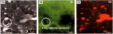
| | Figure 1. Secondary electron image (a) and x-ray maps (b and c) of a nickel alumina composite. | Focused Ion Beam Techniques The focused ion beam instrument is similar in principle to a scanning electron microscope. However, instead of using an electron beam to irradiate the sample, a beam of gallium ions is used. The instrument consists of the ion beam source, a set of electrostatic lenses and a scanning system, which allows the ion beam to be scanned over the surface of the sample with nanometer precision. The technique can be used to mill away the surface of a sample to produce a smooth surface plane with a precision that cannot be obtained using conventional mechanical polishing techniques. The instrument can also be used to mill away bulk areas of a sample to leave a thin section, which can be lifted out of the sample for transmission electron microscopy (TEM) studies. This technique has been used in the semiconductor industry for many years for quality control purposes, but has recently been applied to TEM studies on a variety of mineral specimens. Analysis after Focussed Ion Beam Milling Figure 2a shows the plane surface of a nickel alumina sample. The surface was created using a Hitachi FB-2000A FIB system, which produces a Ga ion beam with accelerating voltages from 10-40kV and beam currents up to 30nA, at 40kV. Milling has removed the surface topography, and in order to enhance the contrast between the nickel particles and the alumina substrate, backscattered electron imaging has been used. | 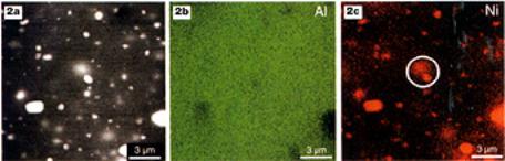
| | Figure 2. Backscattered electron image (a) and x-ray maps (b and c) of a nickel alumina composite after milling a plane surface. | Although the nickel particles closer to the surface are clearly visible, the penetration effects of the electron beam means that there are still a number of particles with indistinct outlines. This is caused by the detection of electrons from nickel particles lying just below the surface of the sample. Although reducing the accelerating voltage would eliminate this effect, there would be insufficient energy to excite the Ni-K aline for X-ray mapping. Figures 2b and 2c show the alumina and nickel in green and red respectively at high accelerating voltage. Some particles are sharply defined but the subsurface ones get increasingly fuzzy (see area circled in figure 2c). High-Resolution X-Ray Analysis One way of overcoming this problem is to prepare a thin section of the area of interest in situ using the FIB milling technique. First the specimen is milled to create a flat plane. Then a gap is box milled in the bulk of the specimen behind the area of interest as shown in figure 3. Further etching from the front using a technique known as local area thinning produces a 100nm thick section for analysis. The electron beam can then pass through the area of interest without any deeply embedded subsurface particles affecting the resolution of the image, figure 4. | 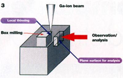
| | Figure 3. Schematic of the focussed ion beam milling procedure. | | 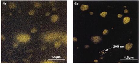
| | Figure 4. X-ray map of a nickel alumina composite before (a) and after (b) ion beam milling. | 3-D Reconstruction In addition to producing high-resolution X-ray maps, the FIB milling technique can also be used to produce 3-D images of the sample so that the dispersion of nickel particles in the alumina matrix can be visualised. The process involves using low volt age backscattered electron imaging. Since no X-ray data is being collected for this application, the accelerating voltage can be reduced to eliminate the penetration effects, but the contrast between the nickel and alumina is retained, ensuring that the nickel particles are easily seen. The technique involves milling a flat surface before recording a backscattered electron image in the S-4700. The sample is returned to the FB-2000A and the surface is milled again to remove a layer of around 0.1 microns thick. The sample is then imaged again in the SEM. The procedure is repeated until around 30 successive images of the sample surface have been acquired. These images can then be processed to create a 3-D image, as shown in figure 5. The 3D reconstructions were created using Voxblast, a voxel-based 3D rendering program developed at the University of Iowa’s Image Analysis Facility. | 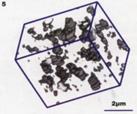
| | Figure 5. 3-D reconstructed image of a nickel alumina composite. | Summary The ion beam milling technique combined with scanning electron microscopy is a powerful method of investigating the microstructures and interpenetrating networks of nickel alumina composites. In addition, the use of the FIB technique to produce ultra-thin lift-out sections suitable for use with high--resolution TEM is also generating a lot of interest. The small sample volumes required make the milling technique one ideally suited to specimens that are unique, precious or small in size. This could include interplanetary dust particles, trace inclusions, or even samples from planetary missions. |