Researchers used 3D model created by AI to understand complex polycrystalline materials that are used in our everyday electronic devices. Image Credit: Kenta Yamakoshi
These materials are extensively employed in information equipment, solar cells, and electronic devices, but the presence of dislocations can diminish the efficiency of such devices.
The study, featured in the journal Advanced Materials, sheds light on the complex nature of polycrystalline materials, which constitute a fundamental component in modern devices ranging from smartphones and computers to the metals and ceramics found in automobiles.
The intricate structures of polycrystalline materials, along with their composition, are challenging to work with. The performance of these materials is influenced by factors such as complex microstructures, dislocations, and impurities. A significant obstacle in the industrial application of polycrystals is the emergence of minuscule crystal defects triggered by stress and temperature fluctuations.
These defects, known as dislocations, can disrupt the regular atomic arrangement in the lattice, consequently impacting electrical conduction and overall performance. To mitigate the risk of failures in devices employing polycrystalline materials, a comprehensive understanding of dislocation formation is crucial.
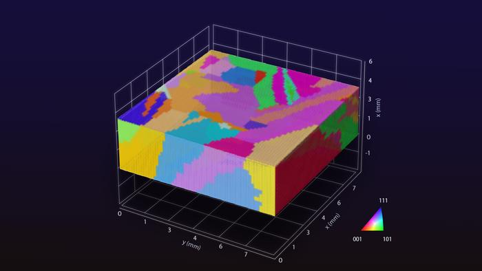
Led by Professor Noritaka Usami, a team of researchers at Nagoya University, including Lecturer Tatsuya Yokoi and Associate Professor Hiroaki Kudo, collaborated on utilizing cutting-edge artificial intelligence to analyze image data of polycrystalline silicon—a widely used material in solar panels. The AI generated a 3D virtual model, facilitating the identification of areas where dislocation clusters were influencing the material's performance.
Once the areas of dislocation clusters were pinpointed, the researchers employed electron microscopy and theoretical calculations to unravel the mechanisms behind their formation.
The study revealed stress distribution in the crystal lattice and identified staircase-like structures at the boundaries between crystal grains, which seemed to be responsible for inducing dislocations during crystal growth.
We found a special nanostructure in the crystals associated with dislocations in polycrystalline structures.
Noritaka Usami, Professor, Nagoya University
In addition to its practical applications, this research holds significant implications for the fields of crystal growth and deformation.
The Haasen-Alexander-Sumino (HAS) model, a prominent theoretical framework employed to comprehend the behavior of dislocations in materials, may not have accounted for certain dislocations, as suggested by Usami.
A subsequent revelation emerged when the team conducted calculations on the atomic arrangement within these structures. Surprisingly, they discovered considerable tensile bond strains along the edges of the staircase-like structures, which played a pivotal role in initiating dislocation generation.
As experts who have been studying this for years, we were amazed and excited to finally see proof of the presence of dislocations in these structures. It suggests that we can control the formation of dislocation clusters by controlling the direction in which the boundary spreads.
Noritaka Usami, Professor, Nagoya University
Usami added, “By extracting and analyzing the nanoscale regions through polycrystalline materials informatics, which combines experiment, theory, and AI, we made this clarification of phenomena in complex polycrystalline materials possible for the first time.”
“This research illuminates the path towards establishing universal guidelines for high-performance materials and is expected to contribute to the creation of innovative polycrystalline materials,” continued Usami.
Usami concluded, “The potential impact of this research extends beyond solar cells to everything from ceramics to semiconductors. Polycrystalline materials are widely used in society, and the improved performance of these materials has the potential to revolutionize society.”
Journal Reference
Yamokoshi, K., et al. (2023) Multicrystalline Informatics Applied to Multicrystalline Silicon for Unraveling the Microscopic Root Cause of Dislocation Generation. Advanced Materials. doi.org/10.1002/adma.202308599.