A new study led by the University of Bristol and published in the journal Nature Electronics highlighted a major breakthrough in semiconductor technology.
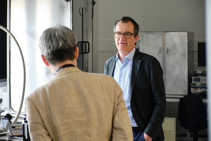
 Image shows Professor Martin Kuball at the Centre for Device Thermography and Reliability (CDTR), based at the University of Bristol, which unites scientists from across the world to develop next generation semiconductor electronic devices. Image Credit: University of Bristol
The recent innovation published in the journal highlights the possibility of communicating and transferring massive amounts of data considerably faster than current networks. Physicists have devised a novel method to hasten this process across many users, potentially worldwide.
Within the next decade, previously almost unimaginable technologies to transform a wide range of human experiences could be widely available. The possible benefits are also far-reaching, including advances in healthcare with remote diagnostics and surgery, virtual classrooms and even virtual holiday tourism.
Martin Kuball, Study Co-Lead Author and Professor, University of Bristol
He added, “In addition, there is considerable potential for advanced driver assistance systems to improve road safety and industrial automation for greater efficiency. The list of possible 6G applications is endless, with the limit just being human imagination. So our innovative semiconductor discoveries are hugely exciting and will help drive forward these developments at speed and scale.”
It is commonly known that the transition from 5G to 6G would necessitate a significant improvement in semiconductor technology, circuits, systems, and associated algorithms. For example, the primary semiconductor components involved, namely radio frequency amplifiers made of the wonder conductor Gallium Nitride (GaN), must be much faster, emit more power, and be more dependable.
International scientists and engineers tested a revolutionary architecture, propelling these unique GaN amplifiers to unparalleled heights. This was accomplished by identifying a latch effect in GaN, which enabled substantially higher radio frequency device performance. These next-generation devices use parallel channels, necessitating the usage of sub-100nm side fins, a transistor that regulates the flow of current traveling through the devices.
We have piloted a device technology, working with collaborators, called superlattice castellated field effect transistors (SLCFETs), in which more than 1000 fins with sub-100 nm width help drive the current. Although SLCFETs have demonstrated the highest performance in the W-band frequency range, equating to 75 gigahertz -110 GHz, the physics behind it was unknown.
Dr Akhil Shaji, Study Co-Lead Author and Honorary Research Associate, University of Bristol
He further added, “We recognized it was a latch-effect in GaN, which enables the high radio frequency performance.”
The researchers then wanted to determine the specific location of this impact using ultra-precision electrical measurements and optical microscopy, so that it could be investigated and understood further. After analyzing over 1,000 fins, the researchers pinpointed this effect to the largest fin.
Kuball added, “We also developed a 3D model using a simulator to further verify our observations. The next challenge was to study the reliability aspects of latch effect for practical applications. The rigorous testing of the device over a long duration of time showed it has no detrimental effect on device reliability or performance. We found a key aspect driving this reliability was a thin layer of dielectric coating around each of the fins. But the main takeaway was clear – the latch effect can be exploited for countless practical applications, which could help transform people’s lives in many different ways in years to come.”
The next phases of the study include improving the devices' power density, which will allow them to provide even better performance and serve a wider range of audiences. Industry partners will also introduce such next-generation products to the commercial market.
Researchers at the University of Bristol are pioneering efforts to improve electrical performance and efficiency in various applications and environments.
Professor Kuball directs the Centre for Device Thermography and Reliability (CDTR), which creates next-generation semiconductor electronic devices for net-zero, communications, and radar technologies. It also enhances device thermal management, electrical performance, and reliability by utilizing broad and ultra-wide bandgap semiconductors.
Journal Reference:
Kumar, A. S. et al. (2025) Gallium nitride multichannel devices with latch-induced sub-60-mV-per-decade subthreshold slopes for radiofrequency applications. Nature Electronics. doi.org/10.1038/s41928-025-01391-5