A new machine learning framework maps how ALD conditions shape hafnium oxide film quality, pointing toward faster, data-driven optimization for next-generation semiconductor fabrication.
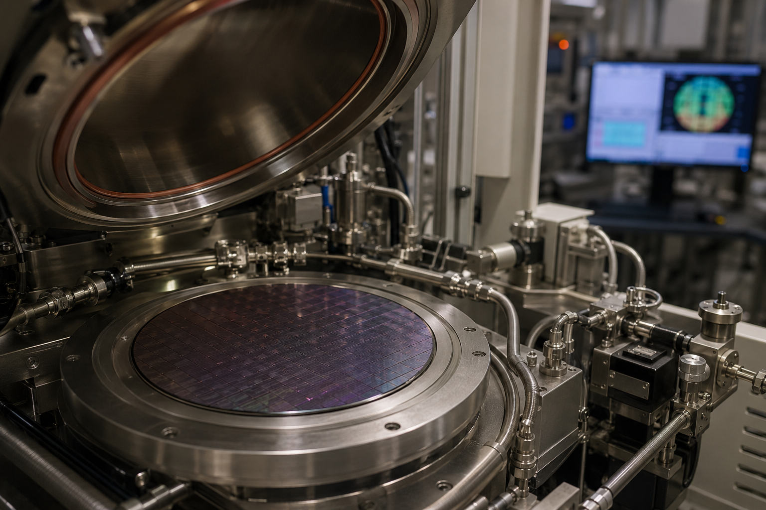
Paper: Machine learning-guided optimization of atomic layer deposition process. Image Credit: AI-generated image / OpenAI
A recent study in the journal Communications Materials presents a machine learning-guided framework for optimizing atomic layer deposition (ALD) of hafnium oxide (HfOx) thin films. The research employs a deep neural network (DNN) to predict key film properties directly from ALD process and wafer-location inputs. The model achieves high prediction accuracy while generating process-property maps that reveal deposition trends and support data-driven process optimization.
Machine Learning-Guided Optimization of Atomic Layer Deposition
As semiconductor devices continue to shrink and adopt increasingly complex three-dimensional architectures, manufacturers face growing challenges in optimizing thin-film deposition processes. Atomic layer deposition (ALD) plays a central role in advanced semiconductor fabrication because it delivers excellent conformality and precise angstrom-scale thickness control.
However, ALD process optimization remains difficult due to the strong interactions among multiple parameters, including deposition temperature, precursor conditions, and reactor environment. Machine learning (ML) has emerged as a promising tool for process development; most previous ALD studies have focused primarily on predicting film thickness. Film thickness provides only limited insight into overall film quality, which is also influenced by factors such as density, optical properties, and etch resistance.
Researchers developed an ML framework that simultaneously predicts film thickness, refractive index, and wet etch rate (WER). The model links ALD process variables to multiple indicators of film quality. As a result, it supports more efficient process development and lays the groundwork for future digital twin technologies.
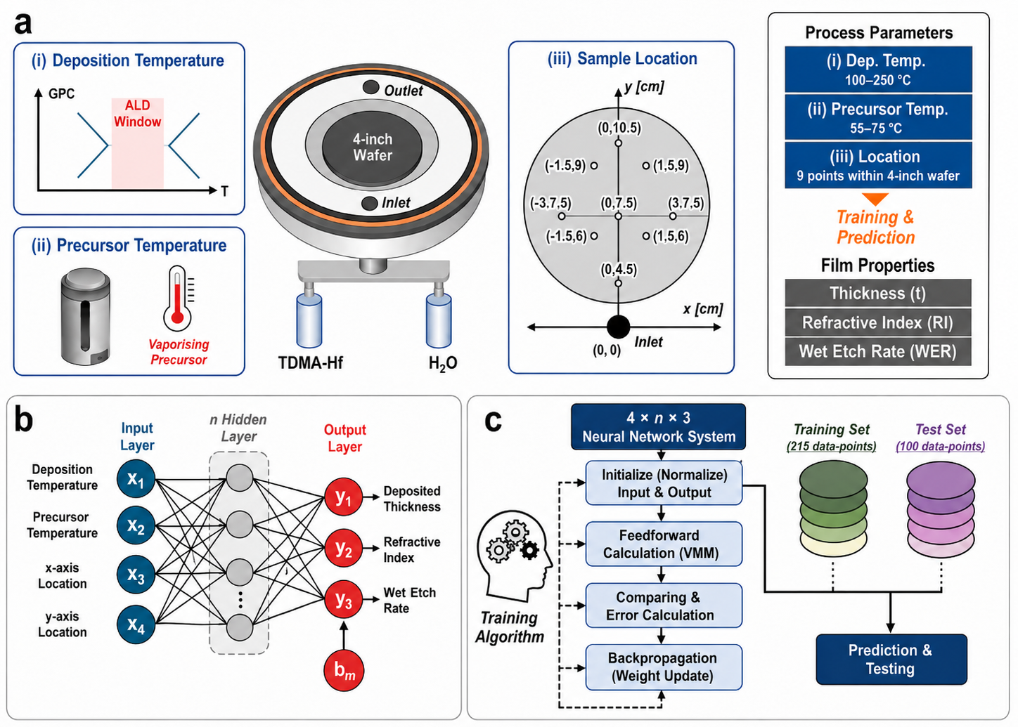
Schematics of the ALD process and deep neural network (DNN) framework for HfOx film deposition. a Controlled ALD process parameters for DNN-driven optimization: (i) deposition temperature, (ii) precursor temperature for TDMA-Hf, and (iii) sample location coordinates on a 4-inch wafer. The process parameters and film properties of interest are displayed on the right. b DNN architecture with 4 input neurons representing ALD parameters and 3 output neurons for film properties. c Training and testing algorithm for the multi-layer NN system, utilizing 215 data points for training and 100 data points for testing. Image Credit: Adapted from Lee, M., Kim, D.S., Chu, T.T.H., et al. (2026). Machine learning-guided optimization of atomic layer deposition process. Communications Materials. DOI: 10.1038/s43246-026-01206-w. Licensed under CC BY 4.0.
Experimental Design and Deep Learning Framework
The researchers developed and validated a machine learning framework using hafnium oxide (HfOx) films deposited by ALD. They used tetrakis(dimethylamido)-hafnium (TDMA-Hf) as the hafnium precursor and water as the oxidant. Experiments took place in a commercial ALD reactor under carefully controlled conditions. The team varied three key process parameters: deposition temperature, precursor temperature, and sample location across a four-inch silicon wafer.
The team collected 315 data points, of which 215 were used to train the ML model, and 100 were reserved for independent testing. The DNN used four input parameters and predicted three output properties: film thickness (Tox), refractive index (RI), and WER. The network comprised five hidden layers with 128, 64, 32, 16, and 8 neurons, respectively. The team also employed an exponential linear unit activation function to improve learning efficiency and prediction accuracy.
The researchers measured thickness and refractive index using spectroscopic ellipsometry. They determined the wet etch rate through controlled hydrofluoric acid etching experiments. Because dense films resist chemical attack more effectively, WER provided an indirect measure of atomic packing density and structural quality. The researchers integrated all experimental data into a structured training and validation workflow to assess model accuracy, robustness, and predictive capability.
High-Accuracy Prediction and Process Visualization
The experimental results highlighted the challenges associated with optimizing ALD processes. When the researchers varied a single process parameter, they observed clear and predictable trends in film properties. Increasing the deposition temperature reduced film thickness and wet etch rate while increasing the refractive index. These changes indicated more complete surface reactions and the formation of denser films.
Changes in precursor temperature also influenced film growth, although the effect stabilized once the precursor reached sufficient vapor pressure for reliable delivery to the substrate surface. The behavior became considerably more complex when multiple process variables interacted. Variations in sample position across the wafer affected precursor transport, reaction kinetics, and local growth rates.
These interactions created nonlinear relationships between process conditions and film properties. One-factor-at-a-time optimization could not fully capture these interdependencies. The DNN learned these complex patterns and accurately predicted film behavior across a wide range of conditions. The model demonstrated strong predictive performance during validation. Cross-validation tests achieved prediction accuracies of 92–95% for film thickness, 95–97% for refractive index, and 90–95% for wet etch rate.
The researchers generated continuous process-property maps that captured key ALD trends. The maps reproduced the overall trends and gradients observed in experimental results across a wide range of deposition conditions. They maintained a strong qualitative trend capture even with a limited training dataset, though quantitative accuracy declined somewhat with fewer training points. This capability allows researchers to identify optimal process conditions more efficiently. The model also generated exploratory predictions beyond the measured experimental space, offering useful direction for future process exploration, but the authors emphasized that such extrapolations should be interpreted cautiously and constrained by ALD process knowledge.
Toward Digital Twin-Guided ALD Development
This study highlights the potential of ML to accelerate semiconductor process development. The researchers combined ALD process parameters with multiple film-quality metrics to build a predictive optimization framework. The model accurately predicted film thickness, refractive index, and wet etch rate. This approach provided a better assessment of film performance than many previous ALD-focused machine learning studies.
The framework generated process-property maps that visualized the relationships between process conditions and film characteristics. These maps helped researchers identify optimal operating windows and evaluate trade-offs among different performance metrics. The current framework focuses on a specific HfOx ALD process and does not yet extend across different deposition systems, facilities, tools, or chemistries.
Future research could adopt physics-guided machine learning approaches that integrate data-driven predictions with established ALD process knowledge. Such approaches may improve model interpretability, strengthen prediction reliability, and enhance performance beyond the measured process space. Overall, the study demonstrates how artificial intelligence (AI) could accelerate ALD process development and support future digital twin platforms for semiconductor manufacturing.
Download your PDF copy by clicking here.
Disclaimer: The views expressed here are those of the author expressed in their private capacity and do not necessarily represent the views of AZoM.com Limited T/A AZoNetwork the owner and operator of this website. This disclaimer forms part of the Terms and conditions of use of this website.
Source:
Lee, M., Kim, D. S., et al. (2026). Machine learning-guided optimization of atomic layer deposition process. Communications Materials. DOI: 10.1038/S43246-026-01206-W, https://www.nature.com/articles/s43246-026-01206-w