Researchers probe how nanoscale silver stressors reshape the metal–MoS2 interface to tackle one of the toughest barriers facing 2D transistors.
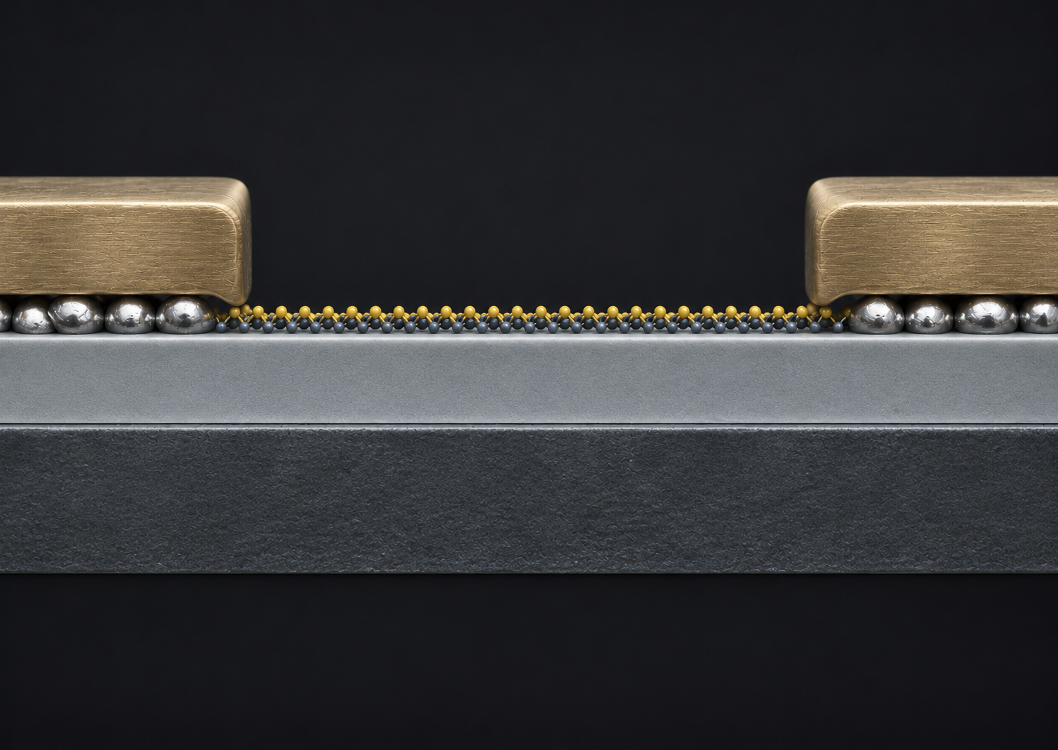
Paper: Contact-localized, strain-engineered metal contacts in 2D field-effect transistors: enabling low-barrier injection via a local stressor. AI-generated abstract conceptual image created using ChatGPT/OpenAI
*Important notice: This news reports on an unedited version of an accepted paper and is awaiting final editing. Therefore, the paper should not be regarded as conclusive or treated as established information.
A recent study published in npj 2D Materials and Applications demonstrates a new approach to improving electrical contacts in molybdenum disulfide (MoS2) transistors through localized strain engineering.
The researchers introduced silver (Ag) nanoislands beneath the source and drain electrodes to generate tensile strain at the metal–semiconductor interface. The findings offer a promising strategy for developing high-performance transistors based on two-dimensional semiconductors.
Addressing Contact Resistance in Two-Dimensional Transistors
Two-dimensional (2D) semiconductors such as MoS2 offer potential for future electronic devices. Their atomically thin channels provide strong electrostatic control, making them suitable for transistors with increasingly smaller dimensions.
However, electrical contacts remain a major obstacle to improving device performance. At the metal–semiconductor interface, a Schottky barrier restricts charge carrier injection and increases contact resistance.
Strain engineering provides a promising way to address this challenge.
Tensile strain expands the atomic lattice and modifies the electronic band structure of a semiconductor. At the contact interface, these changes can shift the conduction-band edge and lower the effective Schottky barrier for electron injection. Applying strain across an entire device can also affect the transistor channel, potentially altering carrier mobility, threshold voltage, and other electrical properties.
To avoid those channel effects, the researchers developed an approach that confines tensile strain to the contact region. They investigated how metal selection, interfacial spacing, and surface morphology influence strain transfer to MoS2.
Engineering Metal Stressors for Localized Strain Generation
The researchers grew monolayer MoS2 films on aluminum oxide substrates predominantly using metal-organic chemical vapor deposition at 600 °C, with additional MoS2 layers covering parts of the surface. They then transferred the films onto device substrates and patterned them to form transistor channels.
To identify suitable stressor materials, the team screened about 20 metals using density functional theory (DFT) calculations. The calculations examined lattice mismatch and equilibrium interlayer distances at different metal/MoS2 interfaces. This analysis helped identify metals that could generate tensile strain while maintaining a non-reactive van der Waals (vdW) interface.
They evaluated work of adhesion, spreading behavior, and adatom surface diffusion, which influence how deposited metal atoms arrange themselves on MoS2. These properties affect whether the atoms aggregate into discrete nanoislands or form continuous films.
Silver (Ag), gold (Au), and aluminum (Al) were selected for experimental comparison, and their surface morphologies were examined using scanning electron microscopy (SEM) and transmission electron microscopy (TEM).
The researchers combined four-dimensional scanning transmission electron microscopy (4D-STEM), grazing-incidence X-ray diffraction (GIXRD), Raman spectroscopy, and X-ray photoelectron spectroscopy (XPS). These techniques allowed them to examine local lattice distortion, average strain, vibrational changes, and interfacial chemistry.
The researchers then fabricated dual-gate MoS2 field-effect transistors (FETs) with a 5 nm Ag stressor beneath the gold source and drain contacts. They also prepared control devices without the Ag layer. Temperature-dependent electrical measurements and the transfer length method allowed the team to evaluate the Schottky barrier height and contact resistance.
How Silver Nanoislands Modify Strain and Electrical Transport
The screening and experimental comparison identified Ag as the most suitable stressor. Ag, Au, and Al could all interact with MoS2 through vdW interfaces, but their growth behaviors differed considerably.
Among these three metals, Ag atoms had the highest calculated surface diffusion coefficient, allowing them to move readily across the MoS2 surface and aggregate into discrete nanoislands. Au formed granules, while Al produced a more continuous film.
Raman spectroscopy revealed pronounced strain-related redshifts only in Ag-deposited MoS2, supporting the role of the Ag nanoisland morphology in generating tensile strain.
Microscopy and diffraction measurements provided evidence of this localized strain. The spacing between the MoS2 (110) crystal planes, or d-spacing, increased from 2.78 Å in pristine regions to 2.82 Å beneath Ag nanoislands, corresponding to local lattice expansion of about 1.4%.
The 4D-STEM strain maps showed that tensile strain concentrated beneath the nanoislands and gradually decreased toward the surrounding MoS2. GIXRD measurements showed that average microstrain across the film increased from 0.08% in pristine MoS2 to 0.2% after Ag deposition.
The extent of strain transfer also depended on Ag thickness and morphology. Discrete nanoislands produced pronounced Raman redshifts, while increasing the Ag thickness caused the islands to merge into a continuous film.
The authors note that localized surface plasmons around Ag nanoislands can partly amplify the Raman signal and increase the apparent Raman-derived strain, though the spectral shifts still support tensile strain.
XPS measurements revealed no detectable chemical bonding, oxidation, charge transfer, or interfacial reactions in MoS2. These results support a mechanical rather than chemical origin for the observed strain.
The Ag stressor was then incorporated into MoS2 transistors to investigate its effect on electrical performance. Temperature-dependent measurements showed that the effective Schottky barrier height decreased from about 100 meV in control devices to about 50 meV in stressor-integrated devices. The transfer length method also showed that contact resistance decreased from 2.2 to 1.5 kΩ μm, a reduction of around 30%.
For representative devices with a 40 nm channel, the on-current increased from about 200 to 320 μA μm-¹, a gain of about 60%.
The stressor-integrated devices also maintained higher on-current across channel lengths ranging from 40 to 500 nm, with the relative gain becoming more pronounced at shorter channel lengths.
The barrier data represent mean values from about 50 devices, and more than 50 devices were measured at each channel length for the resistance and on-current analyses.
These results support contact-localized tensile strain as a way to improve carrier injection while minimizing strain in the transistor channel.
Advancing Contact Engineering for Future 2D Electronics
Taken together, the measurements show that localized mechanical strain can serve as a contact-design variable in two-dimensional transistors.
Tensile strain was generated directly at the metal/MoS2 interface by introducing Ag nanoislands beneath the source and drain electrodes. The electrical measurements associate this contact-localized strain with a lower effective Schottky barrier, reduced contact resistance, and improved carrier injection while preserving the chemical integrity of the semiconductor.
The study identifies three design factors when selecting metal stressors: sufficient lattice mismatch to generate strain, an appropriate interlayer distance to maintain mechanical coupling without strong chemical hybridization, and a nanoisland morphology that concentrates stress near the island edges.
The authors note that practical device integration will require attention to additional factors. The measured Ag nanoisland dimensions are comparable to scaled contact dimensions, suggesting that discrete Ag nanoislands could be used in scaled contact structures. Contact-localized strain adds another design parameter for developing high-performance 2D electronic devices.
Disclaimer: The views expressed here are those of the author expressed in their private capacity and do not necessarily represent the views of AZoM.com Limited T/A AZoNetwork the owner and operator of this website. This disclaimer forms part of the Terms and conditions of use of this website.
Source:
- Yoo, J. E., Hu, L., et al. (2026). Contact-localized, strain-engineered metal contacts in 2D field-effect transistors: enabling low-barrier injection via a local stressor. npj 2D Materials and Applications. DOI: 10.1038/s41699-026-00753-7, https://www.nature.com/articles/s41699-026-00753-7