Non-destructive measuring instruments are required for the characterization of graphene to determine its properties. Confocal Raman-AFM is an ideal instrument for the analysis of nanomaterials. Physical dimensions of nanomaterials can be determined using an AFM, while their molecular composition can be determined using Raman imaging.
Hence, using confocal Raman microscopy in conjunction with an AFM can directly link the high spatial and topographical resolution obtained with an AFM to the molecular information acquired by confocal Raman spectroscopy. The representative results presented in this article demonstrate the ability of the alpha300 RA confocal Raman-AFM microscope system (Figure 1) to perform non-destructive characterization of graphene.
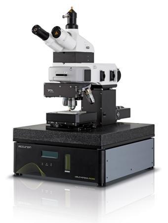
Figure 1. The alpha300 RA confocal Raman-AFM microscope system.
Imaging of Multilayered Graphene
Figure 2 depicts the white light image (a), the AFM topography image (b), and the Raman image (c) of a graphene flake, all obtained with an alpha300 RA microscope, without disturbing the sample between the different measurements. The deposition of the graphene flake on the oxide top layer of a Si-wafer was done by exfoliation. The white light image (Figure 2a) is useful for the coarse analysis of the Si-wafer after deposition of graphene.
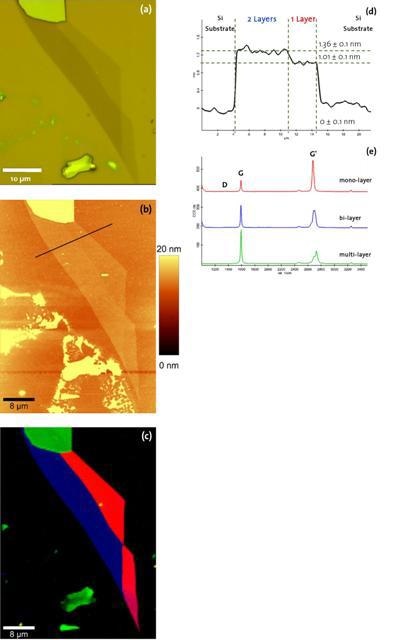
Figure 2. (a) White light image of a graphene flake on a silicon surface. (b) AFM topography image (AC-mode) of graphene, (c) Color coded Raman image. (d) Height profile along the cross section indicated in Figure 2b (black line). (e) Raman spectra measured at different positions of the graphene flake (colors correspond to Figure 2c).
AFM imaging of the same graphene flake was made possible thanks to the accurate cantilever positioning capabilities of the alpha300 RA. The AFM topography image (Figure 2b) shows the 3D-physical dimensions of the graphene flake. The black line Figure 2b represents the cross section of a height profile, which reveals the topography variation over a bi-, mono-, and no graphene layer.
The height difference between the first graphene layer and the oxide Si-substrate 1 ± 0.1nm, whereas for the double layer of graphene, the height difference is 1.36 ± 0.1nm (Figure 2d). This topographic cross section is helpful in highlighting differences of Raman bands as a function of the count of graphene layers. Figure 2e shows the characteristic Raman spectra for a mono-bi-, and multi-layer of graphene as well as the unique D, G, and G' Raman bands of carbon nanomaterials.
Analysis of the Raman bands of Carbon Nanomaterials
In addition to creating Raman images of graphene flakes, the WITec data analysis software provides useful algorithms for an in-depth analysis of 2D Raman spectral arrays. According to a study with a WITec alpha300 R microscope, the Raman spectra of graphene yield accurate data on the electronic band structure, crystal structure, the electron-phonon interaction in sp2 carbon systems, and the phonon energy dispersion.
By observing the integrated intensity, width, position and line shape of the Raman features of the graphene layers, it is possible to probe the thermal conductivity, the strain, the defects, the doping, the crystal orientation, the linear dispersion of electronic energy, and the number of layers. Fitting a Lorenzian curve to the G band reveals a shift towards lower wave numbers, with an increase in the number of graphene layers (Figure 3).
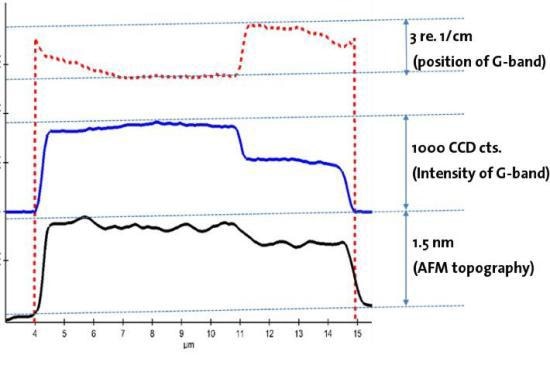
Figure 3. Variations in G-band position and G-band intensity in comparison with the height profile of the AFM topography image.
As shown in Figure 4a, the G' band is represented by a single Lorenzian fit for exfoliated graphene monolayer. However, for double and multilayer of graphene, four Lorenzian curves are needed for the fit of this Raman band (Figures 4b and 4c). This indicates the interplane phonon interaction.
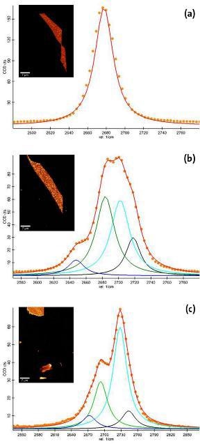
Figure 4. Line shape of the G'-band and Lorenzian fit of the 2D spectral array for (a) monolayer, (b) bi-layer, (c) multilayer of graphene.
Chirality Analyses of Graphene
Figure 5a illustrates the integrated intensity of the D-band across the cross section marked in Figure 2b, along with the height profile from the AFM topography image. This demonstrates that the D-band appears only in spectra acquired at the edge of the graphene flake, not in the spectra for mono- and bi-atomic graphene layers. The corresponding Raman spectra from the graphene flake edges are depicted in Figure 5b, with a highlighted D-band.
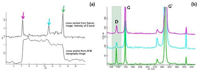
Figure 5. (a) Comparison of D-band intensities with the height profile along the cross section indicated in Figure 2b. (b) Raman spectra from the positions marked in Figure 5a.
A majority of the graphene flakes have edge angles as multiples of 30°. An edge angle of 60° or 120° has the same chirality, while edges with angles of 30°, 90° or 150° show different chiralities (zigzag or armchair) between two adjacent edges (Figure 6a). The results of the analysis of the differences in the intensity of the D-band are provided in Figure 6b, delineating the different angles and chiralities of the graphene flake under analysis. These results demonstrate the advantage of using the confocal Raman-AFM in the design and characterization of new optoelectronic devices, based on the exotic optical, magnetic and superconductive properties of graphene edges.
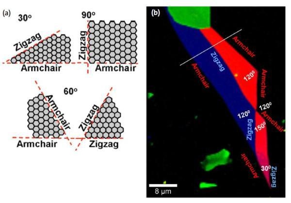
Figure 6. (a) Examples of graphene layer angles and their corresponding chiralities. (b) Determination of the edge chirality (zigzag or armchair).
Figure 7 illustrates the results of a confocal Raman AFM analysis of a CVD graphene layer deposited on a Si substrate. The AFM topography image reveals the presence of defects in form of wrinkles, which appear topographically beyond the surrounding and follow a diagonal direction in the image. The 5x5µm2 higher resolution reveals that the graphene layer is composed of two domains, with a length of 4-5µm and width of 2µm and oriented in diagonal direction and surrounded by cracks in the graphene layer (Figure 7a).
Figure 7c depicts the color coded Raman image of the 10x10µm2 confocal Raman measurement, where as Figure 7b shows the overlay of the AFM and Raman images. The red areas in the Raman image are associated with I(G)/I(G') ratios of 0.2, related to a single layer of graphene (Figure 7d). The blue areas are related to an high I(D)/I(G) ratio, showing high structural defects in the graphene layer (Figure 7e). The yellow and green colors are related to the cracks between the domains (Figures 7F and 7g, respectively).
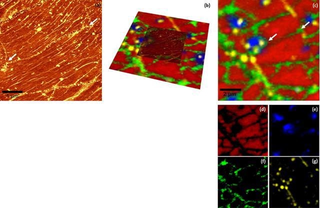
Figure 7. Results of a confocal Raman AFM analysis of a CVD graphene layer deposited on a Si substrate.
The comparison of the high resolution AFM image (Figure 7a) with the color coded Raman image (Figure 7c) reveals that the two graphene domains with wrinkles observed in the AFM image appear in the Raman image as they are surrounded by the defected structure. It is possible to identify the high resolution topographic structures with the observed spectral features (white arrows).
Conclusion
The study results clearly demonstrate the ability of the alpha300 RA confocal Raman-AFM microscope system to perform nondestructive characterization of graphene.

This information has been sourced, reviewed and adapted from materials provided by WITec GmbH.
For more information on this source, please visit WITec GmbH.