|
The Atomic Force Microscope (AFM) has evolved from an extremely high resolution scientific research instrument into a highly accurate metrology tool. This evolution has broadened the role of the AFM from the research bench to the industrial workplace. As the need to examine the ever shrinking geometries of the semiconductor interconnections involved in the chip making process, the extension of the optical imaging system to the nanotechnical realm of the AFM is a logical one.
Atomic Force Microscope (AFM) Surface Sensing
The AFM employs a system of sensing the extremely small differences between the atomically sharp silicon probe and surface under investigation. This sensitivity is essential in monitoring and measuring the nanometer sized surface detail.
Optical systems are able to identify features of interest down to approximately 1 micrometer of separation, but are unable to make an accurate measurement of a feature, or to tell if it is a particle or a divot.
Semiconductor Defect Detection
Figure 1 shows an AFM tip pointing toward an unknown feature on a line of a semiconductor IC. The AFM is able to track the surface and identify a possible defect.
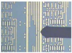
Figure 1. AFM tip pointing toward an unknown feature on a line of a semiconductor IC.
Figure 2. shows an AFM probe during its initial scan to cover the area of interest in Figure 1. The laser light can be seen reflecting from the cantilever sensor to accurately place the probe in the correct vertical position.
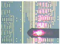
Figure 2. AFM probe during its initial scan to cover the area of interest.
A defect in the edge of a line on the IC circuit is shown in Figure 3. The dark colors are placed at the lowest part of the sample depth, while the brighter colors are placed at the highest point in the topography.
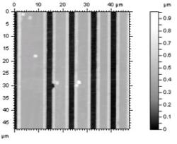
Figure 3. A defect in the edge of a line on the IC circuit.
The Line Profile Analysis in Figure 4 displays show the vertical dimensions along one chosen scan line from the 512 taken during the scan.
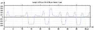
Figure 4. Line Profile Analysis.
A reduced scan "zoom" of a small area of interest is shown in Figure 5. The darkness of the feature and resulting line profile cross-section report that there is a small amount of material missing from the metal line.
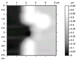
Figure 5. A reduced scan "zoom" of a small area of interest.
A measurement that is used to calculate the volume and area of the missing feature to estimate that amount of material loss that might find its way into the manufacturing process as contamination is shown in Figure 6. The area of the defect is approximately 2.05 um2 and the volume of material that might be missing is 0.134 um3.
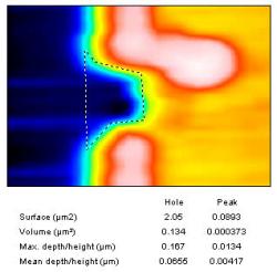
Figure 6. A measurement used to calculate the volume and area of the missing feature to estimate that amount of material loss that might find its way into the manufacturing process as contamination.
Three dimensional reconstruction of the multiple single line profiles from the AFM is shown in Figure 7. The defect is clearly visible in this color enhanced and rotated representation of the lines of the IC interconnect. Some of the material that is missing from the defect may be piled up on the surface, as seen in the red topped bump to the left of the half moon shaped notch in the line edge.
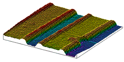
Figure 7. Three dimensional reconstruction of the multiple single line profiles from the AFM. The defect is clearly visible in this color enhanced and rotated representation of the lines of the IC interconnect.
The combination of a fast optical inspection and the AFM's ability to make a quick and accurate measurement help to solve and eliminate problems in the nanotechnological realm.
|