Jul 26 2008
Smaller and faster are two goals in today’s electronics market and an article in an international trade publication shows how North Dakota State University researchers, Fargo, design and build such electronics packages.
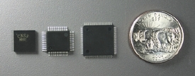 A two-stack chip scale package on the far left designed at North Dakota State University's Center for Nanoscale Science and Engineering is shown next to the two larger packages it replaced, all considerably smaller than a quarter.
A case study by researchers in the Center for Nanoscale Science and Engineering (CNSE) at North Dakota State University was published in the July 2008 issue of the Chip Scale Review magazine. “Case Study: Building a Two-Chip Stacked Package” is authored by Fred Haring, research technician; Chris Hoffarth, engineering technician; Syed Sajid Ahmad, manager of engineering services; John Jacobson, senior design engineer; and Aaron Reinholz, associate director of electronics technology. CNSE staff members Linda Leick, Darci Hansen, Matt Sharpe and Meridith Bell also contributed significantly to the project.
With the increasing demand for more functionality and smaller size with portable devices such as cell phones, mp3 players, and GPS units, the performance and size of individual electronic components have become critical. The case study details how CNSE researchers design and manufacture a chip scale package. Engineering a single package housing multiple chips stacked vertically one on top of the other results in smaller and more efficient packages for devices. For example, CNSE researchers have successfully reduced the size of two electronics components by 75 percent.
Two or more processors packaged in a single package will result in an overall package size smaller than each individual package, yet will have the combined computing power of the two individual integrated processors. The case study walks through this two-chip stacked package process at CNSE, discussing stacked-die design considerations, substrate limitations, stack configuration, assembly process, process documentation, wire bonding, laser marking, ball attaching, singulation, inspection, testing, and hallmark successes of system completion.
For more information on electronics, click here.