Feb 17 2010
The use of germanium instead of silicon as basic material of transistors would enable faster chips containing smaller transistors. However, a number of problems still have to be solved. Transistors are produced using foreign atoms that are implanted into the semiconductor material so that it becomes partly conducting. As this production step damages the material, it has to be repaired by subsequent annealing.
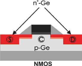 The figure shows schematically the application of germanium in a CMOS (complementary metal oxide semiconductor) circuit. Note that germanium is only used in the regions of source (S), drain (D) and channel (C). Source and drain contain high concentration of foreign atoms (dopants) which provide the excess of free electrons (n+ regions) or holes (p+ regions).
So far it has not been possible to produce large-scale integrated transistors of a specific type (NMOS) using germanium. The reason: phosphorus atoms are strongly redistributed within the material during annealing. Two novel techniques, which were applied by scientists of the research center Forschungszentrum Dresden-Rossendorf (FZD) and international colleagues, overcome this dilemma.
Higher switching speeds than in silicon could be achieved using germanium and some other semiconductors. Germanium is particularly attractive since it could be easily integrated into existing technological processes. Germanium was the basic material of first-generation transistors before it was replaced by silicon at the end of the 1960s. This was due to the excellent electronic properties of the interface between the semiconductor silicon and its insulating and passivating oxide. However, this advantage cannot be utilized if transistor dimensions are further reduced since the oxide must then be replaced by so-called high-k dielectrics. This again stimulates science and industry to search for the most suitable basic material.
By inserting foreign atoms the conductivity of semiconductors can be varied in a purposeful way. One possibility is ion implantation (ions are charged atoms) with subsequent heat treatment, which is called annealing. Annealing of the germanium crystal is necessary as the material is heavily damaged during implantation, and leads to the requested electronic properties. While these methods allow for the manufacturing of p-channel transistors (PMOS) according to future technology needs (22 nanometer technology node), it was not possible to produce corresponding n-channel transistors (NMOS) using germanium. This is due to the strong spatial redistribution (diffusion) of the phosphorus atoms which have to be used in manufacturing the n+ regions.
Physicists from the FZD applied a special annealing method that enables repairing the germanium crystal and yields good electrical properties without the diffusion of phosphorus atoms. The germanium samples were heated by short light pulses of only a few milliseconds. This period is sufficient in order to restore the crystal quality and to achieve electrical activation of phosphorus, but it is too short for the spatial redistribution of the phosphorus atoms. The light pulses were generated by the flash lamp equipment which was developed at the research center FZD. Analysis of the electrical and structural properties of the thin phosphorus-doped layers in germanium was performed in close collaboration with colleagues from the Belgian microelectronics center IMEC in Leuven and from the Fraunhofer-Center for Nanoelectronic Technologies (CNT) in Dresden.
An alternative method to suppress phosphorus diffusion in germanium has been investigated by an international team consisting of researchers from Germany, Denmark and the USA, amongst them physicists from FZD. After ion implantation of phosphorus into germanium the sample was heated to a given temperature and then irradiated by protons. It could be demonstrated that this treatment leads to the reduction of phosphorus diffusion, too. The results of these experiments are explained by the influence of certain lattice defects (self-interstitials) that annihilate those lattice defects (vacancies) which are responsible for the mobility of the phosphorus atoms.
Thus, FZD physicists and their colleagues demonstrated that in principle it is possible to fabricate germanium-based n-channel transistors (NMOS) with dimensions corresponding to the most advanced technological requirements.