Aug 23 2010
The generation of an electric field by the compression and expansion of solid materials is known as the piezoelectric effect, and it has a wide range of applications ranging from everyday items such as watches, motion sensors and precise positioning systems. Researchers at McGill University's Department of Chemistry have now discovered how to control this effect in nanoscale semiconductors called "quantum dots," enabling the development of incredibly tiny new products.
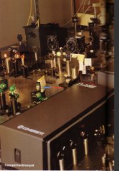 A laser in Dr. Kambhampati's lab that is used to shine light on quantum dots.
Although the word "quantum" is used in everyday language to connote something very large, it actually means the smallest amount by which certain physical quantities can change. A quantum dot has a diameter of only 10 to 50 atoms, or less than 10 nanometres. By comparison, the diameter of the DNA double-helix is 2 nanometres. The McGill researchers have discovered a way to make individual charges reside on the surface of the dot, which produces a large electric field within the dot. This electric field produces enormous piezoelectric forces causing large and rapid expansion and contraction of the dots within a trillionth of a second. Most importantly, the team is able to control the size of this vibration.
Cadmium Selenide quantum dots can be used in a wide range of technological applications. Solar power is one area that has been explored, but this new discovery has paved way for other nanoscale device applications for these dots. This discovery offers a way of controlling the speed and switching time of nanoelectronic devices, and possibly even developing nanoscale power supplies, whereby a small compression would produce a large voltage.
"The piezoelectric effect has never been manipulated at this scale before, so the range of possible applications is very exciting," explained Pooja Tyagi, a PhD researcher in Professor Patanjali Kambhampati's laboratory. "For example, the vibrations of a material can be analyzed to calculate the pressure of the solvent they are in. With further development and research, maybe we could measure blood pressure non-invasively by injecting the dots, shining a laser on them, and analyzing their vibration to determine the pressure." Tyagi notes that Cadium Selenide is a toxic metal, and so one of the hurdles to overcome with regard to this particular example would be finding a replacement material.
The research was published in Nano Letters and received funding from the Canada Foundation for Innovation, the Natural Sciences and Engineering Research Council of Canada, and the Fonds Québécois de la Recherche sur la Nature et les Technologies.