Mar 20 2019
Besides foldable smartphones, the industry’s leading players are also keen on developing flexible displays. So far, touchscreens have been inflexible and do not bend to the anatomical shapes of its wearers. They work as they have good conductive structures close to their surfaces. When the fingers of the user wipe them or tap on them, electronically readable capacities alter. For curved surfaces like conductive tracks are applied to flexible materials, for example, plastic foils. Standard processes for this are laborious or expensive as they either involve a number of process steps or require substantial quantities of raw materials or costly raw materials.
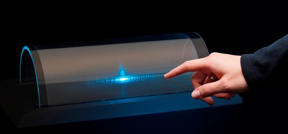 Image credit: INM
The INM—Leibniz Institute for New Materials has formulated new processes using photochemical metallization and printing (inkjet printing and gravure printing) of transparent conductive oxides (TCOs), which are significantly more time-and cost-saving. These will be showcased by the researchers at the 2019 Hannover Messe between 1st and 5th April at Stand C54 in Hall 5.
“Most processes for conductor paths are subtractive: metal is first applied over the entire surface and the excess metal is removed in further process steps. These classic processes, such as sputtering in a high vacuum and subsequent lithography, consume large amounts of silver,” explains Peter W. de Oliveira, head of the InnovationCenter at INM. “Our processes go the other way round: Conductor tracks are printed or deposited only where they are needed. Expensive high-vacuum technology is not needed for this. This new additive process saves time and money,” de Oliveira recapitulates the benefits of the latest developments.
In photochemical metallization, colorless silver compounds are transformed into electrically conductive silver with the help of a photoactive layer when exposed to UV light. UV lasers are used to “write” conductive tracks; UV-transparent photomasks or transparent stamps, which mechanically move the silver compound, are appropriate for larger-scale applications. This renders it possible to down-scale the conductive paths to a width of just one thousandth of a millimeter.
In another groundbreaking process, researchers use nanoparticle inks with TCOs such as indium tin oxide (ITO), for gravure or inkjet printing.
We use the TCOs to produce nanoparticles with special properties. The TCO ink is then produced by adding a solvent and a special binder. Not only does it ensure that the TCO nanoparticles adhere well to the film, it also increases the flexibility of the TCO coating: this ensures that the conductivity is maintained when the films are bent. This makes it possible to produce highly flexible transparent conductor structures, for example for touch sensors or displays, in a simple printing process.
Peter W. de Oliveira, Head of InnovationCenter, INM
The coating is efficient after it has been cured at low temperatures below 130 °C with UV light.