A new imaging technique allows the nano-precise mapping of perovskite cells in 3D.
 Three-dimensional mapping of electrical behavior in perovskite films. Image Credit: NIMTE
Researchers at the Ningbo Institute of Materials Technology and Engineering (NIMTE) have presented a novel three-dimensional (3D) electrical imaging technique that directly illustrates the functioning of defect passivation treatments in perovskite films. The study was published in Newton.
Perovskite solar cells are an attractive alternative to traditional silicon photovoltaics due to their cost-effectiveness and high efficiency. However, the defects present in perovskite films hinder charge transport, leading to energy loss and reduced operational stability.
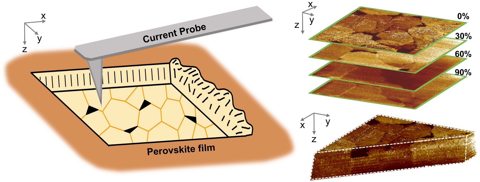
One potential solution is "passivation treatment" – a method that incorporates chemicals such as simple salts or organic molecules into the film. These small molecules or ions attach to the defects in the perovskite material, preventing these defects from disrupting electrical flow. Confirming the internal efficacy of various passivation treatments is difficult, though, as most characterization techniques only examine the surface or yield averaged macroscopic data.
The new technique uses tomographic conductive atomic force microscopy (TC-AFM) to visualize the distribution of current across perovskite films by sequentially removing ultrathin layers of the film while assessing local electrical conductivity at various depths. By compiling these measurements, a three-dimensional map of charge transport within the film can be reconstructed with nanoscale precision.
The researchers analyzed the internal electrical characteristics of perovskite films subjected to different passivation techniques. Untreated films displayed extensive regions of low conductivity that impeded charge transport.
In contrast, bulk passivation significantly diminished these resistive areas within the film, especially along grain boundaries. Surface passivation mainly improved conductivity near the upper interface – a crucial aspect for device integration. The scientists found that films treated with both bulk and surface passivation exhibited the most uniform and continuous conductive pathways, with the remaining low-conductivity regions largely restricted to the surface.
These microscopic electrical characteristics are closely correlated with the resulting solar cell performance, establishing a direct link between 3D charge transport within the film and overall device efficiency.
Chuanxiao Xiao, Professor and Study Corresponding Author, Ningbo Institute of Materials Technology and Engineering (NIMTE), Chinese Academy of Sciences (CAS)
The study presents a direct, three-dimensional perspective on the migration of charge carriers within perovskite films, serving as a valuable resource for assessing and enhancing passivation techniques.
This approach facilitates the systematic design of superior perovskite materials, which in turn promotes the development of more efficient and stable perovskite solar cells, while also contributing to the progress of various thin-film electronic and optoelectronic devices.
Journal Reference:
Li, M., et al. (2026) Three-dimensional mapping of electrical behavior in perovskite films using tomographic conductive atomic force microscopy. Newton. DOI: 10.1016/j.newton.2025.100367.