Simulations suggest buried acoustic waves could turn strained germanium into a compact quantum bus, linking distant qubits without piezoelectric transducers.
Paper: Quantum phononic links for on-chip long-range coupling of hole spin qubits in compressively strained germanium on silicon. Image credit: AI-generated image created using ChatGPT/OpenAI
In a recent research article published in the journal APL Quantum, researchers at the University of Warwick, UK, introduced Quantum Phononic Links (QPLs), an architecture that uses compressively strained germanium on silicon (cs-GoS) and is designed to support scalable, coherent, long-range coupling of hole-spin qubits via engineered phononic waveguides and cavities.
Quantum Phononic Link Concept
Scalable quantum computing using semiconductor spin qubits demands coherent coupling between qubits separated by distances beyond immediate neighbors. Among candidate platforms, hole spin qubits in cs-GoS are especially compelling due to their long coherence times, strong spin–orbit interaction, and compatibility with CMOS fabrication processes.
However, existing long-range coupling approaches, such as charge shuttling, surface acoustic waves (SAWs), and microwave resonators, face footprint and coherence limitations that can constrain their scalability in practical large-scale quantum architectures. This study proposes Quantum Phononic Links (QPLs), an on-chip coupling strategy in which phonons are confined predominantly within the cs-Ge quantum well and guided through an engineered heterostructure.
"One of the key challenges in quantum computing is long-range qubit connectivity," said Dr Maksym Myronov, Department of Physics, University of Warwick. "Our work introduces a new concept in which phonons act as a quantum bus, enabling distant qubits to exchange quantum information while remaining fully compatible with semiconductor technology."
Phonon Confinement Engineering
The QPL concept is modeled using phononic waveguides and cavities formed around the compressively strained Ge quantum well embedded between relaxed Si1−xGex layers. Differences in the layers’ elastic properties and sound velocities produce an acoustic index contrast that favors phonon localization in the lower-sound-velocity material and confines phonons within the Ge QW owing to its lower longitudinal and transverse sound velocities compared to the surrounding Si1−xGex cladding.
This acoustic confinement is further enhanced by the compressive strain, which modulates elastic constants, decreases sound velocity along specific crystallographic directions, and separates transverse modes that would otherwise share the same frequency, improving vertical confinement and mode selectivity. Lithographic patterning provides lateral localization of phonon modes in the QW.
To analyze phonon strain distributions and mode profiles, the authors employed finite-element multiphysics simulations (COMSOL) based on the heterostructure’s elastic properties. In the accompanying theoretical spin-phonon analysis, they used strain tensor components and the relevant valence-band deformation potentials.
The phonons couple to hole spins via the Bir–Pikus Hamiltonian, which captures strain-induced shifts and splitting in valence-band states, including the heavy-hole and light-hole bands. The simulated phonon-induced strain fields would overlap spatially with hole wavefunctions confined electrostatically in gate-defined double quantum dots (DQDs).
The QPL architectures rely on lithographically defined lateral patterning. Shallow etched mesas can provide lateral confinement, while periodic phononic structures, acoustic shields, and mirrors can suppress leakage and isolate selected modes. These approaches are compatible with standard CMOS processes and support controllable frequencies in the gigahertz range.
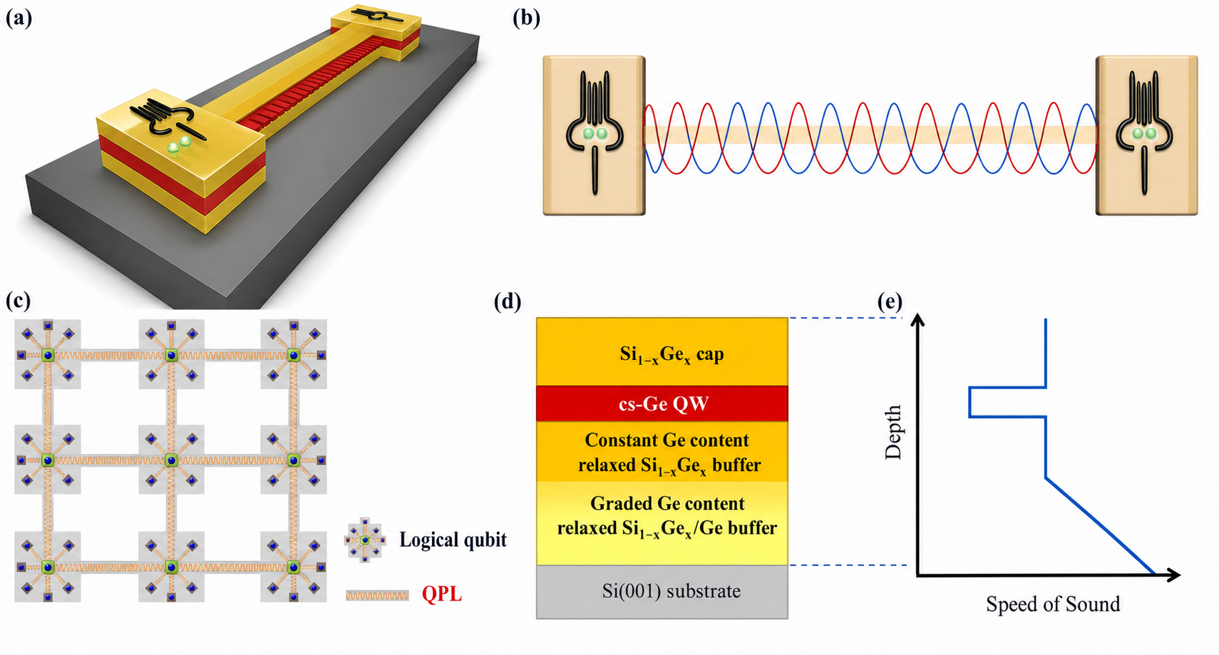
Concept of QPLs for on-chip long-range coupling of hole spin qubits in cs-Ge QW. (a) Three-dimensional schematic of a QPL formed within a cs-Ge quantum well embedded in a Si1−xGex heterostructure, where acoustic phonons are guided along a one-dimensional phononic channel connecting spatially separated qubits. (b) An example of a two-qubit configuration illustrating coherent phonon-mediated coupling between distant gate-defined hole spin qubits formed in DQDs via a confined acoustic mode. (c) An illustration of a multi-node architecture demonstrating scalable phononic interconnects between logical qubits, enabling non-local qubit–qubit interactions beyond direct tunnel coupling. (d) The cs-GoS heterostructure layer sequence used to realize phonon confinement: a cs-Ge QW sandwiched between relaxed Si1−xGex epilayers with engineered acoustic impedance, producing (e) depth-dependent sound-velocity contrast that localizes and guides phononic modes within the cs-Ge QW acoustic channel.
Spin-Phonon Coupling Analysis
Simulations indicate that phononic modes can be engineered and confined tightly within the cs-Ge QW, whose strain fields are expected to modulate hole spin energies via spin–orbit coupling without needing piezoelectric layers or external transducers. Order-of-magnitude calculations placed spin-phonon coupling strengths at approximately 0.1–10 MHz for modes in the 10–50 GHz range, depending on confinement, spatial overlap, and device geometry. These values were not experimentally measured.
The buried acoustic waves (BuAW) exhibit wavelengths on the order of hundreds of nanometers, which are significantly greater than the QW thickness (10–30 nm). Together with acoustic confinement, this scale difference supports strong phonon-spin overlap and coupling.
Simulated strain profiles show that separating the two dots within a DQD by approximately half a wavelength maximizes differential strain and energy detuning between the dots, strengthening the interaction between the qubit and the phononic mode.
The acoustic velocity contrast between the cs-Ge QW and the surrounding Si1−xGex layers provides an effective index-guiding mechanism analogous to that in optical waveguides. However, the study does not demonstrate wafer-scale phonon propagation. Instead, the authors expect current material quality to permit coherent propagation over tens of micrometers to centimeters, while describing potential compatibility with wafers up to 300 mm in diameter.
QPLs offer several potential advantages over conventional qubit-coupling methods. Unlike SAW systems that rely on piezoelectric substrates and interdigital transducers, the QPL approach would integrate the coupling mechanism directly into a non-piezoelectric semiconductor, avoiding additional electric-field noise channels associated with piezoelectric transducers.
The compact footprint of phononic waveguides, at nm to µm scales, would support dense qubit layouts compared with centimeter-scale microwave resonators. The authors propose controlling phononic modes lithographically to achieve frequency selectivity and mode isolation, enabling selective long-range coupling without compromising qubit density.
Challenges such as acoustic scattering from interface imperfections and wafer-scale inhomogeneities are acknowledged. Nonetheless, the authors expect current material quality in state-of-the-art cs-GoS heterostructures to support coherent phonon propagation over tens of micrometers to centimeters, while larger systems would require further phononic band engineering and fabrication advances.
The authors also provide a qualitative comparison describing QPLs as combining direct strain-mediated coupling, buried phonon confinement, and nanometer-to-micrometer footprints, distinguishing the proposed architecture from SAW, phononic crystal, and microwave resonator platforms.
Scalable Quantum Bus Outlook
The research proposes Quantum Phononic Links as a material-native architecture for scalable, long-range coupling of hole-spin qubits in compressively strained germanium on silicon. By confining acoustic phonons within the cs-Ge quantum well and leveraging strain-induced spin–orbit interactions, the proposed QPLs are designed to provide coherent, frequency-selective, and electrically tunable coupling between distant qubits without the need for piezoelectric transducers.
This approach offers a compact, CMOS-compatible pathway to scale up semiconductor quantum architectures while avoiding the electric-field noise associated with piezoelectric transducers. The material-engineered acoustic confinement and strain coupling are intended to enable QPLs to serve as a compact quantum bus integrated directly within the semiconductor heterostructure.
Overall, this work provides a theoretical and simulation-based foundation for investigating larger-scale quantum processors and hybrid quantum networks based on hole spin qubits linked by tailored phononic excitations. Experimental fabrication and testing will be required to verify the predicted coupling strengths, coherence lengths, and scalability.