Users can combine the imaging and analysis power of a high-resolution field emission scanning electron microscope (FE-SEM) with the processing capacity of a next-generation focused ion beam microscope (FIB). They might be at a multi-user facility, an academic or industrial lab, or somewhere different altogether.
Use ZEISS Crossbeam’s modular platform concept to scale up the system as customer needs change, such as with the LaserFIB for large-scale material ablation. Crossbeam will speed up FIB milling, imaging and 3D analytics applications.
- Maximize SEM Insights
- Increase FIB Sample Throughput
- Experience Best 3D Resolution in FIB-SEM Analysis
Highlights
Maximize SEM Insights
- Get true sample information from high-resolution SEM pictures using Gemini electron optics
- Characterize the sample carefully using a variety of detectors. Users may acquire clean materials contrast using the Inlens EsB detector
- Investigate nonconductive specimens that have not been affected by charging artifacts
- Use the ZEISS Crossbeam’s SEM capabilities for 2D surface, sensitive images or 3D tomography
- Tandem decel, a feature of the new ZEISS Gemini electron optics, may boost SEM resolution by up to 30% at low voltage
- Benefit from high resolution, contrast and signal-to-noise ratios even while using very low acceleration voltages

Image Credit: Carl Zeiss Microscopy GmbH
Increase FIB Sample Throughput
- The Ion-sculptor FIB column takes a novel approach to FIB processing: by preventing sample destruction, users may increase sample quality while still finishing studies faster
- When preparing TEM samples, make use of the low voltage capabilities of the Ion-sculptor FIB to get ultra-thin samples with little amorphization damage
- Manipulate samples precisely and fast with up to 100 nA current without affecting FIB resolution
- Make use of advanced FIB scanning methods’ speed and precision for material removal to speed up studies by up to 40%

Image Credit: Carl Zeiss Microscopy GmbH
Experience Best 3D Resolution in FIB-SEM Analysis
- To save time, collect serial section images during milling. For active picture quality control, use trackable voxel sizes and automated algorithms to achieve precision and consistency
- ZEISS Atlas 5, the market-leading package for rapid, precise tomography, may be added to the Crossbeam to improve its capacity
- ZEISS Atlas 5’s integrated 3D Analytics tool enables users to do EDS and EBSD analyses during tomography runs
- The greatest 3D resolution and largest isotropic voxel size in FIB-SEM tomography give unique insights. The Inlens EsB detector can probe to a depth of less than 3 nm and provide material contrast images that are surface sensitive
- Take advantage of the benefits of integrated 3D analysis for EDS and EBSD exams
- Crossbeam will speed up the FIB milling, imaging, 3D analytics and other applications

Image Credit: Carl Zeiss Microscopy GmbH
Crossbeam Family
Crossbeam 350
Perform in situ studies with outgassing or charging samples using the Variable Pressure mode and a low vacuum operation. High-quality imaging and high throughput are provided by the Gemini electron optics and the Ion-sculptor FIB.

Image Credit: Carl Zeiss Microscopy GmbH
Crossbeam 550
Perform the most accurate characterizations possible and choose the chamber size that best suits the samples, whether standard or large. The Gemini 2 electron optics provide excellent resolution even at low voltage and high current. At high beam current, it is ideal for high-resolution imaging and rapid analytics.

Image Credit: Carl Zeiss Microscopy GmbH
Crossbeam Laser
The airlock’s femtosecond laser enhances in situ research, prevents chamber contamination, and can be set as Crossbeam 350 or 550, making it a perfect instrument for massive material ablation and thorough sample preparation. Prepare very tough structures, such as atom probe samples, or gain quick access to structures that are deeply buried.

Image Credit: Carl Zeiss Microscopy GmbH
Correlative Cryo Workflow
Imaging in a near-native state is possible using this cryogenic solution for TEM lamella production and volume imaging. The electron microscopy techniques of widefield, laser scanning and focussed ion beam scanning electron microscopy are all connected. At the same time, maintain the adaptability of a multi-purpose FIB-SEM.

Image Credit: Carl Zeiss Microscopy GmbH
ZEISS Crossbeam Laser Workflow
Access buried sections of interest quickly, run associated workflows across several length scales, improve sample representativity with large-volume analysis, and do 3D imaging and analytics. Benefit from site-specific, ultra-fast sample preparation when a femtosecond laser is added to the ZEISS Crossbeam.
- Benefit from femtosecond laser pulses in a regulated vacuum environment that cause minimum damage and heat impacted zones
- Correlation with previously obtained 3D X-Ray microscopy datasets or other external data might help the user find the deeply buried regions of interest (ROIs)
- Maintain the cleanliness of the FIB-SEM main chamber and detectors by doing laser work in a specialized integrated chamber
- Gain quick access to structures that are buried deep down
- Prepare extraordinarily large cross-sections with widths and depths of up to millimeters
Perform Set-Up Steps for Laser Ablation
- Place the sample on the holder and set it in the main chamber of the FIB-SEM
- In ZEISS correlative workspaces, import, overlay and align 3D X-Ray data or 2D optical microscope pictures, for example
- Determine the ROI and obtain a reference image

Image Credit: Carl Zeiss Microscopy GmbH
Register SEM and Laser Coordinates
- To lock sample and SEM coordinates, scan the four sample holder fiducials with the SEM
- Transfer the sample to the integrated femtosecond laser chamber (fs)
- To lock sample and laser coordinates, scan the four sample holder fiducials with the fs laser
- The coordinates of the SEM and the laser have now been matched

Image Credit: Carl Zeiss Microscopy GmbH
Perform Massive Material Ablation
- Make a laser pattern
- Keep the laser pattern visible
- Rapidly remove large amounts of material with greater than 2 μm targeted accuracy
Top down SEM view. Image Credit: Carl Zeiss Microscopy GmbH

Cross-section SEM view. Image Credit: Carl Zeiss Microscopy GmbH
Transfer the Sample to the Main FIB-SEM Chamber to Continue FIB-SEM Work
- The microstructures may already be seen in detail
- Polish the FIB as needed for high-resolution imaging
- With new procedures, users can make TEM and atom probe samples
- With instant SEM feedback, users can quickly optimize laser recipes

FIB-polished Cross-section SEM view. Image Credit: Carl Zeiss Microscopy GmbH

Cross-section, detail showing the defect. Image Credit: Carl Zeiss Microscopy GmbH
The Workflow for TEM Lamella Preparation
Navigate to the Region of Interest
Almost every FIB-SEM user has to prepare TEM lamellas. For site-specific preparation, ZEISS offers an automated workflow. The resultant lamellae are appropriate for high-resolution TEM and STEM imaging and atomic-resolution analysis.
Navigate to the specimen’s ROI, remove the TEM lamella with ROI from the bulk sample, bulk mill or trench the sample, and finish the procedure with lift-out and thinning as needed.

Navigate to the region of interest. Image Credit: Carl Zeiss Microscopy GmbH
Automated Navigation to the Specimen’s Region of Interest (ROI)
- Begin the workflow without wasting time looking for the ROI
- Locate specimens using the airlock’s navigation camera
- It is simple to get to the ROI thanks to the integrated user interface
- Make use of the SEM’s broad, distortion-free field of view

Image Credit: Carl Zeiss Microscopy GmbH
Automated Sample Preparation (ASP) to Prepare a Lamella Out of the Bulk
- Begin by following a simple three-step procedure: ASP
- Establish the recipe, which should include drift correction, deposition and coarse and fine grinding
- The FIB column’s ion optics allow for great workflow throughput
- Start a batch preparation by duplicating the recipe and repeating it as needed

Image Credit: Carl Zeiss Microscopy GmbH
Lift Out
- Attach the lamella to the tip of the micromanipulator
- Remove the lamella from the bulk of the material
- After that, the lamella is ready to be lifted out and transported to a TEM grid

Image Credit: Carl Zeiss Microscopy GmbH
Thinning: The Final Step is Crucial; It Defines the Quality of TEM Lamella
- The instrument’s architecture allows for achieving the desired lamella thickness by allowing live monitoring of the thinning process
- On the one hand (with the SE detector), use two detector signals simultaneously to assess lamella thickness and get repeatable end thickness; on the other hand, use two detector signals in parallel to check surface quality (with the Inlens SE detector)
- Make high-quality samples with little amorphization

Image Credit: Carl Zeiss Microscopy GmbH
TEM Lamella Preparation and Volume Imaging under Cryogenic Conditions
Cryogenic microscopy allows researchers to examine cellular structures in their natural condition. Users, on the other hand, confront several obstacles, including sample preparation, devitrification, ice contamination, sample loss and correlation across imaging modalities.
Widefield, laser scanning and focussed ion beam scanning electron microscopy are all combined in the ZEISS Correlative Cryo Workflow in a single, simple operation. From fluorescent macromolecule identification to high-contrast volume imaging and on-grid lamella thinning for cryo-electron tomography, hardware and software are tuned for the demands of correlative cryogenic processes.

Components of the ZEISS Cryo Accessory Kit. Image Credit: Carl Zeiss Microscopy GmbH
Imaging the Near-to-Native State
- For cryogenic and ambient temperature applications, it can be used in a variety of ways
- Devitrification and ice contamination prevention for samples
- Fluorescence imaging with high resolution
- The cryogenic process is seamless across several modalities
- Cryo TEM applications need to target on-grid lamella thinning
- Volume imaging with high contrast and 3D reconstruction
A Simplified Workflow to Help Focus on Research
Users conquer the challenging mixing of several imaging modalities under cryo conditions with ZEISS Correlative Cryo Workflow. The workflow solution enables volume imaging and efficient fabrication of TEM lamellae by connecting light and electron microscopy.
Dedicated accessories streamline the workflow and ensure that cryo samples are safely transferred between microscopes. ZEN Connect ensures data management by keeping the data in context throughout the workflow. Several processing tools are available to assist users to improve the image findings.

Image Credit: Carl Zeiss Microscopy GmbH
Superior Components to Give Best-in-Class Data Quality
ZEISS LSM systems enable the user to identify proteins and cellular structures at great resolution using cryo-compatible objectives and the high sensitivity of the Airyscan detector, while soft lighting and consistently low temperatures keep the samples from devitrifying.
With the ZEISS Crossbeam FIB-SEM, users can get high-contrast volumetric imaging even if the materials are not stained with heavy metals. Whether users follow up with TEM investigations or not, both modalities provide essential functional and structural information that can give researchers a full grasp of the ultrastructure.

Image Credit: Carl Zeiss Microscopy GmbH
Multipurpose Solutions to Maintain Imaging Facility’s Productivity
Unlike other systems, the ZEISS microscopes used in the workflow may be used for both cryogenic and room temperature applications, which is especially useful when the microscopes are not being completely employed for cryogenic studies.
It takes only a few minutes to convert the equipment from cryogenic to room temperature operation, and no technical knowledge is required. This adaptability allows users to devote more time to their investigations. Better usage and a faster return on investment are advantages for imaging facilities.

Image Credit: Carl Zeiss Microscopy GmbH
The Technology Behind ZEISS Crossbeam
SEM Electron Optics
Choose Between Two Columns
As with other ZEISS FE-SEMs, the FE-SEM column of ZEISS Crossbeams is based on Gemini electron optics. Choose between Crossbeam 350’s Gemini VP column and Crossbeam 550’s Gemini II column.
High-resolution imaging is the goal of field emission SEMs. The electron optical column of a field emission SEM is critical to its performance. All ZEISS FE-SEMs and FIB-SEMs have Gemini technology, which is designed for exceptional resolution on any sample, particularly at low accelerating voltages, full and efficient detection and ease of use.
Gemini Optics is Characterized by Three Main Components
- Small probe sizes and high signal-to-noise ratios are guaranteed by Gemini beam booster technology, which includes integrated beam deceleration
- By detecting secondary (SE) and backscattered (BSE) electrons in parallel, the Gemini Inlens detection method assures efficient signal detection while reducing time-to-image
- The Gemini objective lens combines electrostatic and magnetic fields to improve optical performance while minimizing field impacts at the sample. This allows for great imaging even on difficult samples like magnetic materials
Benefits for FIB-SEM Applications
- With the use of near magnetic-field free optics, obtain distortion-free, high-resolution imaging even over vast fields of view
- Without affecting the electron-optical performance, tilt the specimen
- The SEM alignment’s long-term stability and the ease with which it modifies all system parameters including probe current and acceleration voltage

ZEISS Crossbeam 350: Gemini column with single condenser, two Inlens detectors and VP capability. Image Credit: Carl Zeiss Microscopy GmbH

ZEISS Crossbeam 550: Gemini II column with double condenser and two Inlens detectors. Image Credit: Carl Zeiss Microscopy GmbH
Crossbeam 350 with Gemini I VP
- Experiments involving outgassing and charging samples in situ
- The Inlens EsB detector contrasts with the unique Gemini substance
- In multi-purpose settings, maximum sample flexibility is required
Crossbeam 550 with Gemini II
- With high-resolution imagery and quick analytics, users can get more information in less time
- With simultaneous Inlens SE and EsB imaging, users may get a unique topographical and material contrast
- The double condenser technique provides good resolution even at low voltage and high current
Gemini Novel Optics
Profit from Surface Sensitive Imaging
As a rule, today’s SEM applications need high-resolution imaging with low landing energy. It is required for:
- Samples that are sensitive to light
- Materials that are not conductive
- Obtaining actual sample surface information without having to deal with unwanted background data from deeper sample layers
Gemini optics are designed for low and extremely low voltage resolutions as well as contrast enhancement. The high gun resolution mode and selectable Tandem decel are technological features.
- As the primary energy width is reduced by 30% in the high gun resolution mode, chromatic aberration is decreased
Tandem decel, now introduced to ZEISS crossbeam 350/550, can be used in two different modes:
- Tandem decel, a two-step deceleration method, combines beam booster technology with a high negative bias voltage delivered to the sample: the primary electron beam’s electrons are decelerated, lowering the landing energy
- Use variable negative bias voltage of 50 to 100 V. The contrast of the images can be improved using one of the application modes
- Improve the low kV resolution of the images by applying a negative bias voltage between 1 and 5 kV

Tandem decel optional sample biasing up to 5 kV further improves the excellent imaging capabilities at low voltages. Image Credit: Carl Zeiss Microscopy GmbH
FIB-SEM Technology
Discover a New Way of FIB Processing
The Ion-sculptor FIB column speeds up the FIB work without sacrificing machining quality, and users may use it on any sample thanks to its low voltage performance.
The Ion-sculptor, a next-generation focused ion beam column from the ZEISS Crossbeam Family, features strong currents for high throughput and exceptional low voltage performance for great sample quality.
- Due to beam currents of up to 100 nA, users may conduct high-throughput tests
- Achieve a FIB resolution of less than 3 nm, which is extraordinary
- Reduce amorphization in specimens and achieve the best possible outcomes after thinning
- For long-term experiments, the Crossbeam series includes automated FIB emission recovery
- Utilize the Ion-sculptor FIB column’s low voltage capabilities to improve sample quality
- With quick probe of current exchanges, users may speed up the FIB applications
- Obtain accurate and repeatable outcomes while maintaining optimum stability

ZEISS Crossbeam 550 with a Gemini II column incl. double condenser and two Inlens detectors and a FIB-column arranged at an inclination angle of 54°. Image Credit: Carl Zeiss Microscopy GmbH
Applications
Material Science


Energy Materials. Lithium-ion battery example, product key featuring cross-sectioning & 3D Tomography and 3D Analysis LiMn2O4 cathode material of a lithium-ion battery. Close-up of cross-section shows surface information on an Inlens SE image A). The distribution of lanthanum (red) and manganese (green) is derived from an EDS map B). Image Credit: Carl Zeiss Microscopy GmbH

Engineering Materials. H-bar lamella preparation by fs-laser on a copper semi-circle grid. The left lamella is 400 μm wide, 215 μm deep and has a thickness of about 20 μm at the top. It was cut by the laser in 34 seconds. The amount of material that needs to be removed by FIB for final thinning is significantly reduced. Image Credit: Carl Zeiss Microscopy GmbH

Engineering Materials. Key feature fs laser machining: Array of compression testing pillars in high entropy alloy, machined fully automatically. Image Credit: Carl Zeiss Microscopy GmbH
Electronics & Semiconductor

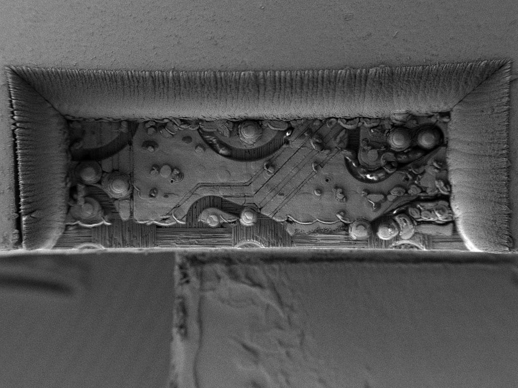
3D-NAND – FIB-SEM Tomography. FIB-SEM tomography dataset acquired from a commercially purchased 3D NAND sample. Sample was de-packaged and mechanically polished down to the topmost word line. Data acquisition was done on ZEISS Crossbeam 550 using ZEISS Atlas 3D. Voxel size 4 × 4 × 4 nm3. Left: 3D rendering of the complete 2 × 4 × 1.5 µm3 volume. Middle: Virtual sub-volume of 2 × 1.5 × 0.7 µm3 size, extracted from the dataset at the transition region of upper to lower deck. Right: Single horizontal slice taken from the volume, showing a top-down view of a word line. Image Credit: Carl Zeiss Microscopy GmbH

Power Electronics – Insulated Gate Bipolar Transistor. Insulated Gate Bipolar Transistor (IGBT) device analysis. The analysis was performed entirely on ZEISS Crossbeam 550. First, a FIB cross-section across the gate electrode was cut, exposing irregularly distributed dark features (top). Second, a lamella was prepared from the left-hand part of that cross-section, and imaged by 30 kV STEM-in-SEM. The brightfield STEM image shown here reveals that the features are crystalline precipitates (bottom). Third, EDS elemental mapping of the lamella showed that the precipitates are silicon (right). Image Credit: Carl Zeiss Microscopy GmbH

3D Stacked Die Interconnect. Crossbeam laser provides fast, high-quality cross-sections of Cu-pillar microbumps buried 760 µm deep with total time to results of <1 hour. Left: 3D integrated circuit (IC) flip chip prepared for microbump imaging with laser ablation and FIB polishing. Right: 25 µm diameter microbump image acquired with backscattered electrons. Image Credit: Carl Zeiss Microscopy GmbH
Life Sciences

Microbiology - Trypanosoma. Ultrastructural investigation of the parasite Trypanosoma brucei. The cells are high pressure frozen and freeze-substituted in EPON. Acquisition of 800 z-sections which corresponds to ~ 8 μm thickness in z; pixel size in x/y is 5 nm. Sample courtesy: S. Vaughan, Oxford Brookes University, Research Group ’Cell biology of Trypanosomes’, UK. Image Credit: Carl Zeiss Microscopy GmbH
Accessories
Visualization and Analysis Software
ZEISS Recommends Dragonfly Pro from Object Research Systems (ORS)
Advanced analysis and visualization software for 3D data gathered using a range of methods such as X-Ray, FIB-SEM, SEM and helium ion microscopy.
ORS Dragonfly Pro is an accessible, full and configurable toolbox for the display and analysis of huge 3D grayscale data, available only through ZEISS. Dragonfly Pro provides access to, annotates and creates media files from the 3D data, including video production. To quantify the results, use image processing, segmentation and object analysis.

Lithium-ion Battery. Image Credit: Carl Zeiss Microscopy GmbH
Introducing ToF-SIMS Enables High Throughput in 3D Analysis
Analyze trace elements, light elements (e.g. lithium) and isotopes with the ToF-SIMS (time of flight secondary ion mass spectrometry) spectrometer attached to the Crossbeam 350 or Crossbeam 550. Benefit from sensitive and thorough 3D evaluations. Perform depth profiling and elemental mapping.
Benefit from simultaneous detection of atomic and molecule ions down to the ppm level, with lateral and depth resolutions of more than 35 nm and 20 nm, respectively. Post-mortem, retrieve any signal from the ROI.

Working principle of SIMS. Image Credit: Carl Zeiss Microscopy GmbH