The ZEISS Sigma family integrates FE-SEM technology with an exceptional user experience. It also enhances efficiency by organizing the imaging and analysis operations. When using an instrument from the ZEISS Sigman family, users will be able to investigate novel materials, particles for quality control, or biological or geological specimens.
Users no longer need to make concessions in high-resolution imaging; instead, they can use low voltages to gain improved resolution and contrast at 1 kV or lower. Use best-in-class EDS geometry to perform advanced analytical microscopy and obtain analytical data at double the speed and with greater precision.
With the Sigma family, users join the world of high-end nano-analysis.
- Sigma 360 is the core imaging facility’s choice — an intuitive FE-SEM for imaging and analytics.
- Sigma 560 uses best-in-class EDS geometry to deliver high throughput analytics and enable automated in situ experiments.
Highlights
Sigma 360 — The Core Facility’s Choice For Intuitive Acquisition
- Get expert guidance from setup to AI-based results. Discover an easy-to-use imaging workflow
- Notice the difference at 1 kV and lower. Improved resolution and contrast can be obtained
- Use extreme VP imaging to produce good results on non-conductors

Polystyrene, imaged with NanoVP lite mode. Image Credit: Carl Zeiss Microscopy GmbH
An Intuitive Imaging Workflow Guides the User from Setup to AI-based Results
- Effective results even for a novice user. With a simple, quick-to-learn workflow, users can expedite each step, from navigation through post-processing, giving a quick time-to-image and saving time during training.
- Software automation in ZEISS SmartSEM Touch starts off with navigation, parameter setup, and image acquisition.
- Then comes the ZEN core, which includes task-specific toolkits and is best suited for post-processing. The AI Toolkit lets the user segment images based on machine learning. Merge multi-modal experiments with the Connect Toolkit. Alternatively, utilize the Materials Apps to examine microstructure, grain size, and layer thickness.

Image Credit: Carl Zeiss Microscopy GmbH
See the Difference at 1 kV and Below — Enhanced Resolution and Optimized Contrast
- The optical column is critical to imaging and analytics performance. Sigma employs ZEISS Gemini 1 electron optics, which enable exceptional resolution on any sample, particularly at low voltages.
- Sigma 360’s low-kV resolution is now set at 500 V with 1.9 nm. By reducing chromatic aberrations, it was possible to enhance 1 kV resolution by more than 10% at 1.3 nm.
- Imaging is now simpler than ever, even on difficult materials and even with backscatter detection in variable pressure (VP) mode.

Image Credit: Carl Zeiss Microscopy GmbH
Accomplish VP Imaging at the Extremes — NanoVP lite Mode for Analytics and Imaging
- The new NanoVP lite mode and detectors make it simple to obtain high-quality data from non-conductors with voltages below 5 kV.
- As a result, imaging and EDS analytics are improved, delivering more surface-sensitive data, faster collection times, and increased primary beam current for faster EDS mapping.
- New detectors, such as the aBSD1 (annular backscatter electron detector) or the C2D (cascade current), provide superb images at low voltage.

Image Credit: Carl Zeiss Microscopy GmbH
Sigma 560 — High Throughput Analytics For Automated in situ Experiments
- Efficient real-world sample analytics: SEM-based investigations that are quick and versatile.
- Automate the in-situ research: Unattended testing in a highly integrated lab.
- Image challenging samples less than 1 kV: Gather extensive sample data.

Image Credit: Carl Zeiss Microscopy GmbH
Efficient Analytics of Real-world Samples — Investigate With Versatility and Gain Speed in EDS
- The best-in-class EDS geometry of the Sigma 560 boosts analytical productivity. Even at low beam current and low acceleration voltage, the two 180° diametrically opposed EDS ports ensure throughput and shadow-free mapping.
- Additional EBSD and WDS ports on the chamber provide analytics beyond EDS.
- With the new NanoVP lite mode, even non-conductors can be investigated with greater signal and contrast.
- The new aBSD4 detector quickly produces images on highly topographical samples.
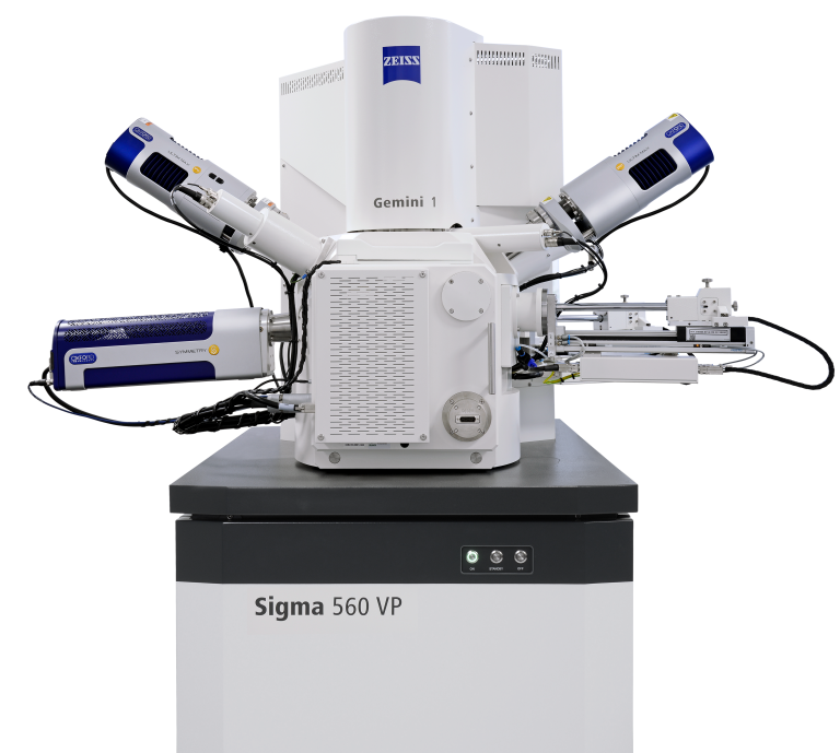
Image Credit: Carl Zeiss Microscopy GmbH
Automate in situ Experiments: A Fully Integrated Lab for Unattended Testing
- The in situ lab for Sigma, a fully integrated solution, allows for operator-independent results of tensile and heating tests in an unattended, automated workflow.
- Enhance the workflow by examining nano-scaled features in 3D: Conduct 3D STEM tomography or AI-based image segmentation.
- The new aBSD4 allows for real-time 3D surface modeling (3DSM).

Image Credit: Carl Zeiss Microscopy GmbH
Image Challenging Samples Easily — See the Difference at 1 kV and Below
- The best imaging and analysis results can be obtained at 1 kV or even 500 V; the low-kV resolution for the Sigma 560 is specified as 1.5 nm at 500 V.
- Easily investigate difficult samples under varying pressure in the new NanoVP lite mode, with acceleration voltages as low as 3 kV and either the new aBSD or C2D detector.
- Maintaining a clean environment is important while researching electronic devices. Safeguard the chamber from contamination with a (highly recommended) plasma cleaner and the new big airlock that allows 6″ wafer shuttling.

Image Credit: Carl Zeiss Microscopy GmbH
Applications
Materials Science
Explore images of various materials samples, including fibers, polymers, molybdenum disulfide, and more.

The surface of a fractured polystyrene sample was imaged to understand crack formation and adhesion at interfaces in polymers. Sigma 560, 3 kV, NanoVP lite mode at 60 Pa chamber pressure, C2D G2. Image Credit: Carl Zeiss Microscopy GmbH

MSC capsules (hollow mesoporous silica) for drug delivery. Backscatter imaging reveals iron oxide core in silica-nanocapsules. Sigma 560, HDBSD, 5 kV. © Courtesy of Dr. V. Brune, Institute of Inorganic Chemistry, University of Cologne, Germany. Image Credit: Carl Zeiss Microscopy GmbH

Carbon nanotubes (CNT) imaged with low voltage. Sigma 560, 500 V, Inlens SE detector. Image Credit: Carl Zeiss Microscopy GmbH

Al2O3 spheres. Terraces of sintered particles are visible under surface-sensitive imaging with high resolution at 500 V. Some distances between terraces are as small as 3 nm. Sigma 560, 500 V, Inlens SE. Image Credit: Carl Zeiss Microscopy GmbH

The surface of a particle from a cathode foil of a battery. Material contrast is used to identify the binder (darker material) on the Li-NMC, imaged with the aBSD. Image Credit: Carl Zeiss Microscopy GmbH

CVD-grown MoS2 2D crystals on Si/SiO2 substrate: The RISE image demonstrates wrinkles and overlapping parts of the MoS2 crystals (green), multilayers (blue) and single layers (red), image width 32 µm. Image Credit: Carl Zeiss Microscopy GmbH
Life Sciences
Understand more about protozoan and fungal micro- and nanostructures, and disclose ultrastructure on block face samples or thin sections.

The delicate open structure of a radiolarian is imaged effortlessly by the ETSE detector at 1 kV under high vacuum , image width 183 µm. Image Credit: Carl Zeiss Microscopy GmbH

Mushroom spores imaged at 1 kV at high vacuum. These delicate, fragile structures can be imaged easily with Sigma 500 at low voltage. Image Credit: Carl Zeiss Microscopy GmbH
Ultrastructure of the bryozoan Tricellaria inopinata, a sessile marine species, field of view 30 µm. Acquired with ZEISS Sigma 560, Sense BSD detector, 1 kV, 30 pA. Image Credit: Anna Seybold and Harald Hausen, Sars Centre for Marine Molecular Biology, University of Bergen, Norway.

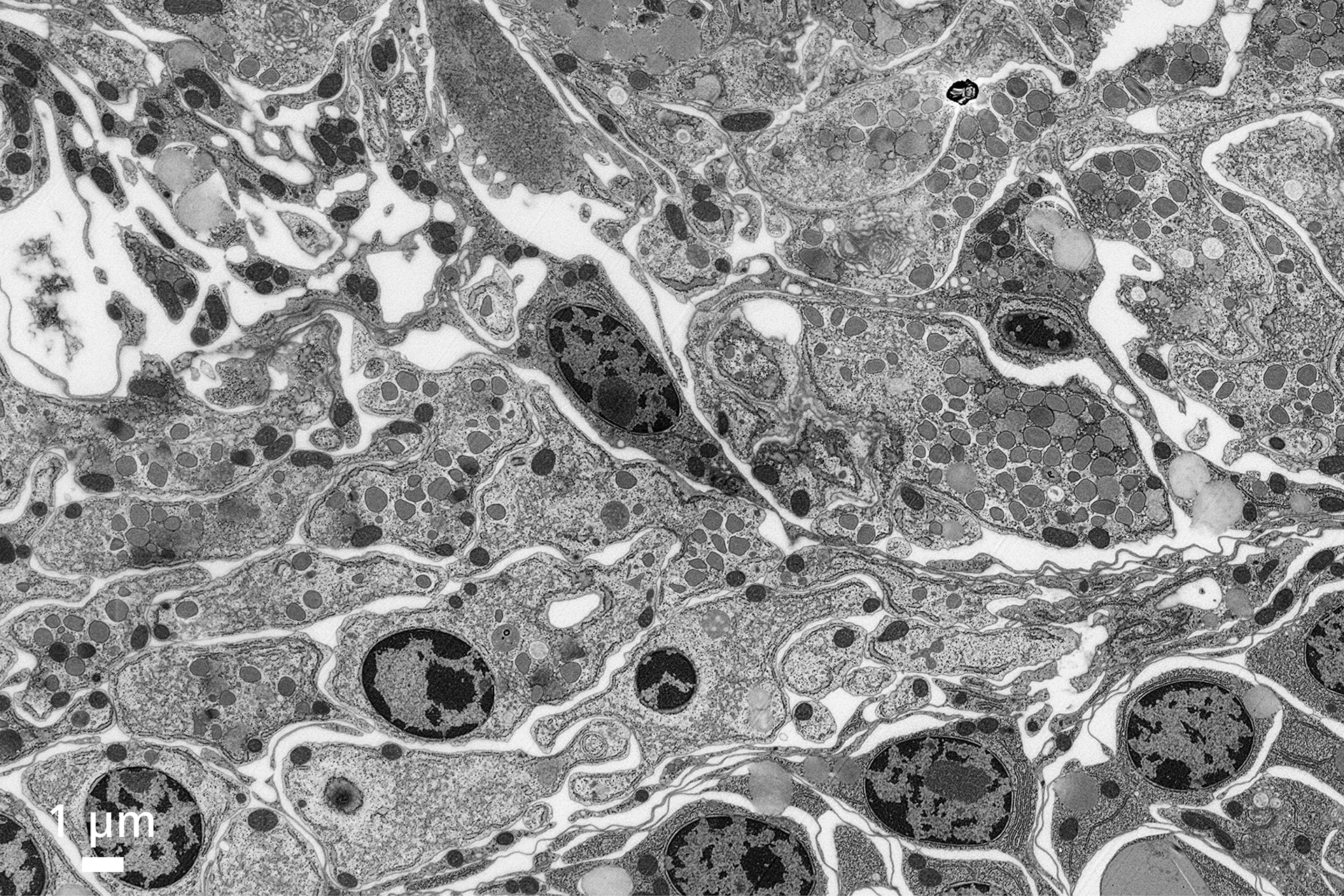
Automatic acquisition of 3D brain ultrastructure using serial block-face imaging. Astrocyte (cyan) was identified and segmented. Image Credit: Dr. Peter Munro and Hannah Armer, UCL Institute of Ophthalmology.
Geosciences and Natural Resources
Investigate metals, rocks, and ores.

Rock sample imaged with the YAG-BSD which delivers images at high speeds due to the performance in light conducting of the YAG crystal, imaged at 20 kV. Image Credit: Carl Zeiss Microscopy GmbH

Nickel sulfide ore. Mineralogic mineral EDS map, image width 3.1 mm. Sample: courtesy of the University of Leicester, UK.

Iron Mineralogy: Raman identification of iron ore mineral, SEM image and Raman maps overlaid. (Hematite is red, blue, green, orange and pink; goethite is light blue). Image Credit: Carl Zeiss Microscopy GmbH

Iron Mineralogy, Raman spectra: Differences in the spectra of hematite are attributed to the different orientations of the crystals. (Hematite is red, blue, green, orange and pink; goethite is light blue). Image Credit: Carl Zeiss Microscopy GmbH

Quantitative EDS major element heatmap (Ca) of garnet-bearing gneiss highlighting geochemical zoning within key minerals. Image Credit: Carl Zeiss Microscopy GmbH
Industrial Applications
Discover how metals, alloys, and powders are analyzed.

Non-conductive titanium dioxide nanoparticles used as pigments and opacifying agents can be imaged easily at 40 Pa in VP mode with the C2D detector, image width 10 µm. Image Credit: Carl Zeiss Microscopy GmbH

25 – 50 nm iron oxide particles imaged with the aSTEM detector in darkfield mode at 20 kV. Image Credit: Carl Zeiss Microscopy GmbH

Superconductor alloy sample imaged at 1 kV with the a BSD. (Scalebar 20 µm). Image Credit: Carl Zeiss Microscopy GmbH

Zinc oxide dendrites: detect morphological changes in the electrodes of energy storage systems. Sigma, ETSE, 5 kV. Image Credit: Carl Zeiss Microscopy GmbH