Jun 22 2009
The new series of Nikon LSI inspection microscopes, Eclipse L200N and L200ND, is now available. Building on the high resolution and precision of the Eclipse L200 and L200D series, the L200N and L200ND offer improved observation and operating performance, providing images with greater contrast and higher resolving power. Used independently or in combination with wafer loaders, the L200 series performs exceptionally precise optical inspection of wafers, photo masks, reticules and other substrates.
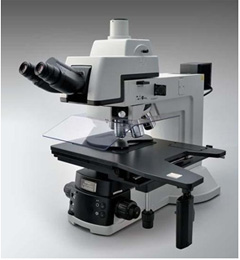
Nikon's original CFI60 optics provide both image brightness through higher NAs, and wider sample range and access with longer WDs. In addition to brightfield, darkfield, simple polarizing and DIC, the episcopic illuminator enables epi-fluorescence observation, including 365 nm UV excitation in the L200ND. With widening inspection capabilities, this is highly beneficial for the observation of semiconductor resist residues and organic electroluminescence displays. High-intensity 12V-50W halogen illumination is brighter than standard 12V-100W illumination at half the power consumption. By incorporating a lamphouse rear mirror and optimising the size of the lamp filament, the user benefits from effective and uniform illumination on the pupil plane, critical in an optical system. Electrostatic discharge coatings have been applied to all parts and controls to safeguard against contamination damage to samples.
Nikon's outstanding proprietary technology ensures that the Eclipse L200N, in combination with the NWL200 wafer loader, offers safe, reliable automated loading of ultra-thin 100µm wafers for inspection.
Featuring an ergonomic design, main controls are located at the front of the base for easy access, allowing stage movements and focusing to be carried out with ease and minimising fatigue during lengthy observations. A tilting trinocular eyepiece tube enables observation at optimum eye level to ensure a comfortable viewing position. Quick and easy microscope operation while viewing samples is possible. The L200N series allows easy and accurate focusing on low-contrast samples, such as bare wafers, simply by inserting a focusing target in the optical path. Up to six objectives can be mounted on the robust motorised nosepiece which also minimises image shifting even between high magnifications.
Control of the camera, peripherals and microscope are all integrated within NIS-Elements imaging software which offers high-quality advanced image acquisition, processing and analysis. Easy USB connection offers high-speed data transfer.