 Non-epitaxial single crystalline 2D materials at wafer-scale. Image Credit: Bae lab
Sang-Hoon Bae, an Assistant Professor of mechanical engineering and materials science at Washington University in St. Louis’ McKelvey School of Engineering, is one of the three researchers who spearheaded the multi-institutional study, which was published in Nature on January 18th, 2023, along with his Doctoral Student Justin S. Kim and Postdoctoral Research Associate Yuan Meng.
The research, which incorporates two technical advancements, is the first to disclose that their methodology of growing semiconductor materials called transition metal dichalcogenides (TMD) might allow devices to run quicker and use less power.
To develop the new materials, the group, co-led by Jeehwan Kim, an Associate Professor of mechanical engineering and materials science and engineering at the Massachusetts Institute of Technology, and Jin-Hong Park, a Professor of information and communication engineering and electronic and electrical engineering at Sungkyunkwan University, had to resolve three immensely challenging issues.
The challenges were securing single crystallinity at the wafer-scale; avoiding irregular thickness during growth at the wafer-scale; and vertical heterostructures at the wafer-scale.
According to Bae, 3D materials undergo a roughening and smoothing process to achieve an even surface. However, 2D materials do not permit this process, resulting in an uneven surface that makes large-scale, high-quality, uniform 2D materials impossible to achieve.
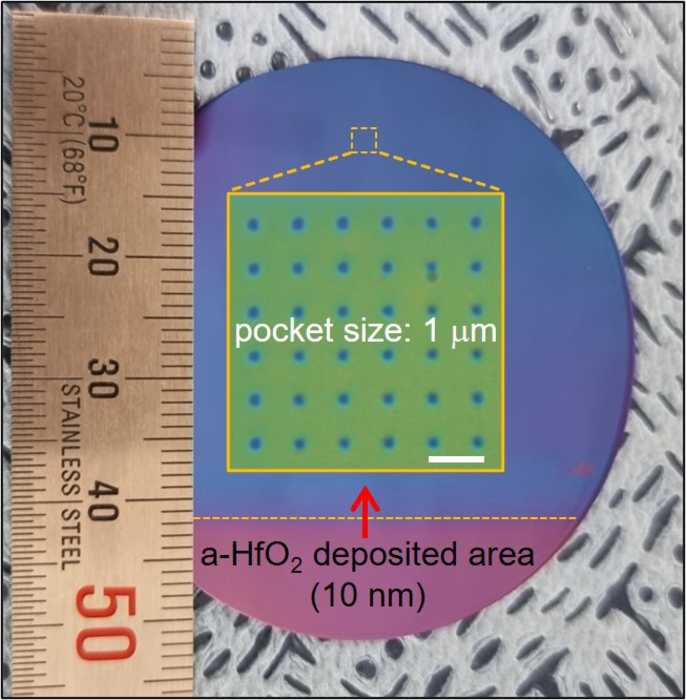
We designed a geometric-confined structure that facilitates kinetic control of 2D materials so that all grand challenges in high-quality 2D material growth are resolved. Thanks to the facilitated kinetic control, we only needed to grow self-defined seeding for a shorter growing time.
Sang-Hoon Bae, Assistant Professor, Mechanical Engineering and Materials Science, McKelvey School of Engineering, Washington University in St. Louis
Another technical breakthrough was demonstrated by the researchers by layer-by-layer growth of single-domain heterojunction TMDs at the wafer-scale, or a large scale. They employed a variety of chemical compound substrates to limit the growth of the nuclei. These substrates developed a physical barrier that hindered the establishment of lateral-epitaxy and promoted vertical growth.
We believe that our confined growth technique can bring all the great findings in physics of 2D materials to the level of commercialization by allowing the construction of single domain layer-by-layer heterojunctions at the wafer-scale.
Sang-Hoon Bae, Assistant Professor, Mechanical Engineering and Materials Science, McKelvey School of Engineering, Washington University in St. Louis
According to Bae, other scientists are exploring this material at sizes as small as tens to hundreds of micrometers.
We scaled up because we can solve the issue by producing the high-quality material at large scale. Our achievement will lay a strong foundation for 2D materials to fit into industrial settings.
Sang-Hoon Bae, Assistant Professor, Mechanical Engineering and Materials Science, McKelvey School of Engineering, Washington University in St. Louis
The study was funded by Intel, DARPA (029584-00001 and 2018-JU-2776), and Institute for Basic Science (IBS-R034-D1).
Journal Reference: