To aid in TEM specimen preparation, the JIB-PS500i offers three solutions. From specimen preparation to TEM observation, a high throughput workflow is guaranteed.
Features

Image Credit: JEOL USA, Inc
TEM-Linkage
The link between the TEM and the FIB is enabled through the application of a double tilt cartridge and TEM holder* from JEOL. The cartridge can be fixed to the exclusive TEM specimen holder with just a single touch.
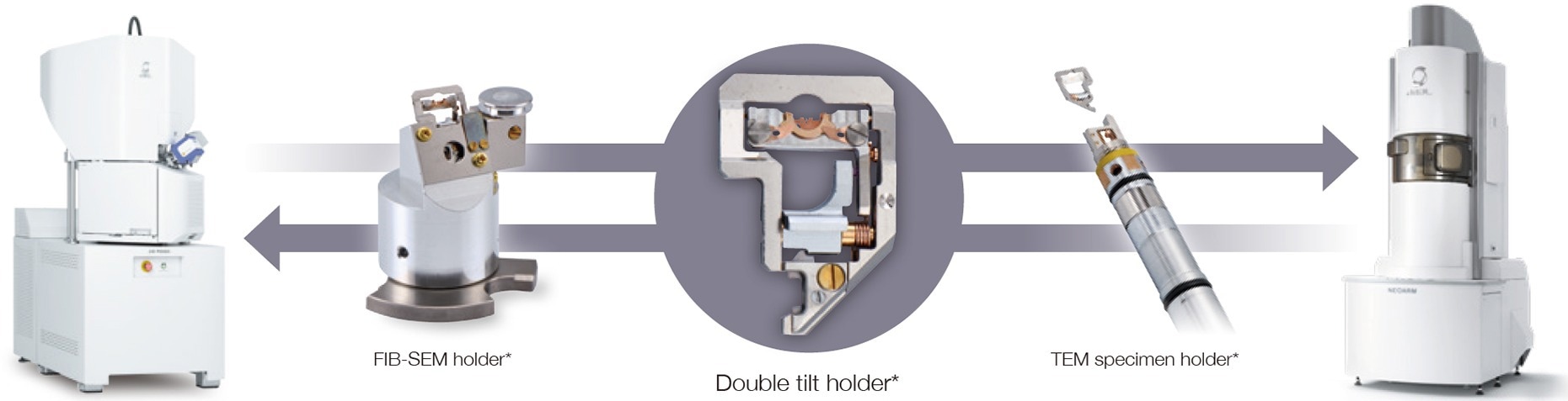
Specimen transfer workflow with the double tilt cartridge*. Image Credit: JEOL USA, Inc
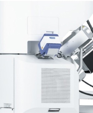
OmniProbe 400*. Image Credit: JEOL USA, Inc
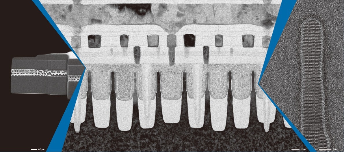
Specimen: 5 nm design rule semiconductor device (FinFET) Observation conditions: (Left) Accelerating voltage 2 kV, Detector SED Secondary electron image, (center and right) Accelerating voltage 200 kV, TEM image, Instrument: JEM-ARM200F. Image Credit: JEOL USA, Inc
The adopted OmniProbe 400* (Oxford Instruments) facilitates accurate and seamless manipulations and pick-up operations. The functions of the OmniProbe 400* are incorporated into the JIB-PS500i’s software.
Check-and-Go
To precisely and efficiently prepare a TEM specimen, it is essential to check in on the preparation progress. Using its high-tilt stage and detector scheme, the JIB-PS500i enables a smooth transition from FIB milling to scanning transmission electron microscope (STEM) imaging. Quick transitions from lamella processing to STEM imaging result in successful specimen preparation.
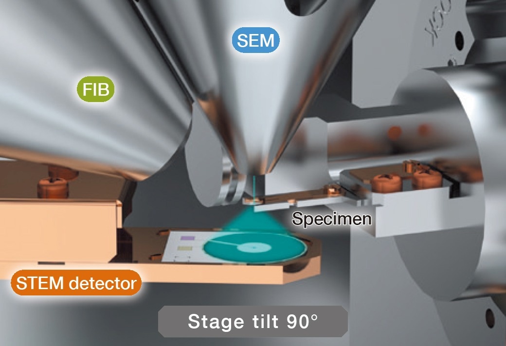
Image Credit: JEOL USA, Inc
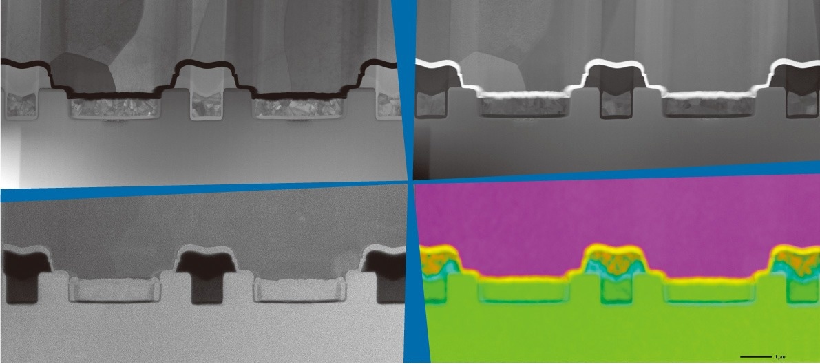
Specimen: SiC power semiconductor device Observation conditions: Accelerating voltage 30 kV, Detector (Upper left) STEM-BF, (Upper right) STEM-DF, (Lower left) SED Secondary electron image, (Lower right) EDS maps Purple: Al Yellow: Ti Orange: P Blue: O Green: Si. Image Credit: JEOL USA, Inc
JIB-PS500i Focused Ion Beam FIB-SEM