Park Systems’ latest atomic force microscopy innovation, the Park FX200, is designed specifically for 200 mm samples. Its sophisticated mechanical structure assures much lower noise levels, minimum thermal drift, and remarkable stability. The FX200 establishes a new benchmark for precision and reliability. Its faster Z servo performance and better high-power sample view improve operating efficiency and imaging capabilities.
Features such as automatic probe detection and exchange, laser beam alignment, and macro optics for complete sample view improve the user experience and productivity. With optical autofocus, navigation, and sequential measurements at several coordinates, the FX200 simplifies complex tasks. It also supports automated AFM scan parameter sets and data analysis, making it an excellent choice for research and industrial applications.
Park FX200, with its enhanced performance and user-friendly design, significantly improves nanoscale imaging and analysis. It empowers scientists and engineers to make meaningful discoveries and drive progress in their work.
Streamline the Research
Park FX200 | The most advanced AFM for samples from small sizes up to 200 mm
Video Credit: Park Systems
Enhanced AFM Core Technology
Lower Noise Floor and Minimal Thermal Drift
The upgraded mechanical structure minimizes operational noise floor and thermal drift, allowing for a more focused SLD beam point that exceeds previous limits. This results in increased measurement accuracy and high-resolution images.
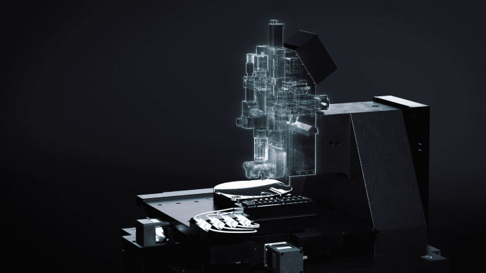
Image Credit: Park Systems
Small Laser Spot Size
- Powered by a high-force piezoelectric stack and directed by a flexure structure
- SLD beam diameter of 11 µm allows for faster imaging with cantilevers
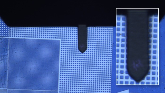
Image Credit: Park Systems
Faster Z Servo Performance
- Guided by a flexure structure and powered by a high-force piezoelectric stack.
- The new FX AFM electronic controller enables faster Z servo performance with more accuracy
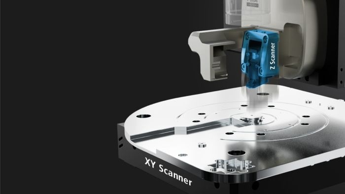
Image Credit: Park Systems
The Most Accurate AFM Scanning Mode Ever
The True Non-contact™ Mode provides unprecedented control over tip-sample distance at the sub-nanometer scale.
The industry’s fastest and most precise non-contact AFM is the Park FX200.
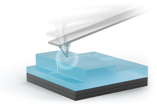
Image Credit: Park Systems
Handles Wafers and Multiple Samples
It is designed for industrial applications and can handle wafers up to a range of sample sizes, including wafers up to 200 mm.
The vacuum chuck can store up to 16 coupon samples, allowing for multiple studies in one setup.
Full 200 mm Wafer Support
Accepts wafers up to 200 mm in size, which is critical for semiconductor fabrication and materials science research. The vacuum chuck provides secure placement for high-resolution imaging and exact measurements, increasing versatility and efficiency.
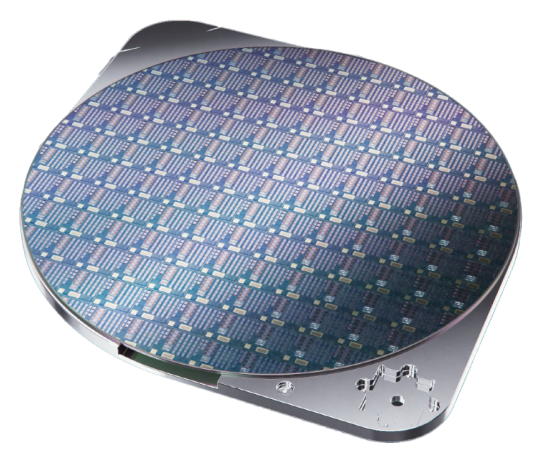
Image Credit: Park Systems
Holds up to 16 Coupon-Sized Samples
The vacuum chuck can hold up to 16 coupon-sized samples simultaneously, increasing productivity by allowing several experiments in a single setup. This function minimizes downtime while increasing efficiency, making it suitable for labs that need to evaluate several samples fast.
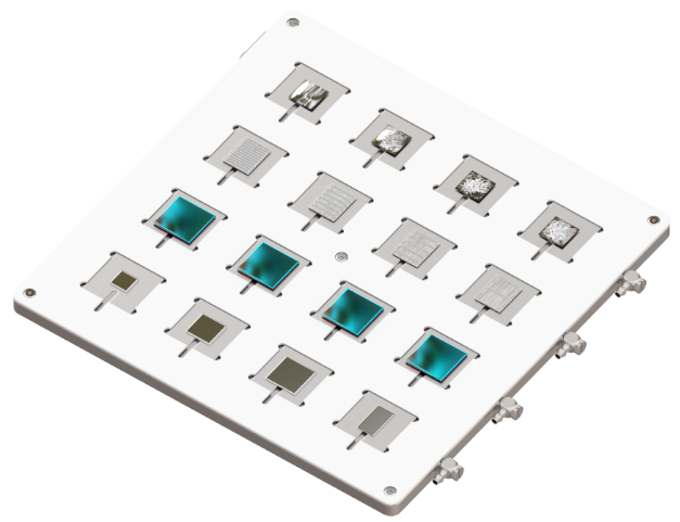
Image Credit: Park Systems
Intelligent Automation
It automates critical processes like probe detection and exchange, laser alignment, and parameter adjustment, increasing efficiency. It has 16 probe slots for repetitive measurements and mode switches, which reduces downtime and increases efficiency.
Automatic Probe Type Recognition
The Probe Identification Camera detects the QR code imprinted on the chip carrier of a new probe. It displays all relevant information about each tip, such as kind, model, application, and usage. This enables the quick selection of the optimal probe tip for each work, assuring precision and efficiency.
Automatic Probe Exchange
Automated probe exchange conveniently and safely replaces outdated probes with full automation. It has 16 probe slots for repetitive measurements and mode transitions, reducing downtime and increasing efficiency through quick, autonomous probe switching.
Automatic Laser Beam Alignment
Automatic Beam Alignment directs the laser beam to the correct location on a cantilever and optimizes the spot’s vertical and lateral position on the PSPD. It automatically moves the X, Y, and Z axes for sharper images with no distortion with the push of a button.
Simplified Operation
Automatic Focus and Navigation
Advanced Region of Interest (ROI) Zooming uses a broad field-of-view sample camera to display the entire 200 mm wafer, making analysis easier by allowing for quick, precise positioning. This decreases the time required to discover target locations, ranging from broad survey scans to specific magnifications. Furthermore, the improved optical vision provides remarkable clarity, resolving line widths below 1 µm.
Automatic Sequential Measurements
It enables automated execution of predetermined coordinate settings on big samples, such as 200 mm wafers or multi-sample chucks. It allows for sequential measurements, including topography and advanced modes, as well as the simplification of workflows in research and industrial applications.
Next-Generation AFM Controller for High-End Products
The Park FX Controller is specifically intended to improve the performance of the Park FX Series. This important advancement enables sophisticated Piezoresponse Force Microscopy (PFM) applications, including Contact Resonance PFM (CR-PFM) and Dual-Frequency Resonance Tracking (DFRT-PFM), without the need for extra hardware. This means the customers can fully benefit from the newest advances in atomic force microscopy.
- DFRT-PFM without external amplifiers
- Improved security and continuous environmental surveillance
- Direct CR-PFM enablement with greater bandwidth for tip bias modulation
- Faster data and image processing with faster Ethernet connectivity
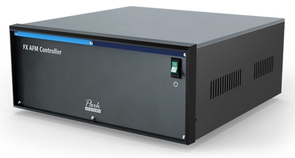
Image Credit: Park Systems
Park AFM-IR Spectroscopy
Advanced Nano-IR Spectroscopy for Large Sample Chemical Analysis
The Park AFM-IR system combines atomic force microscopy (AFM) and infrared (IR) spectroscopy. Chemical identification is provided via the spectroscopic portion with a spatial precision of 5 nm.
It employs a non-contact method with the highest industry spatial resolution and the safest spectroscopy scanning. The microscopy portion gives users information on mechanical properties and nanoscale 3D topography with sub-angstrom height accuracy.
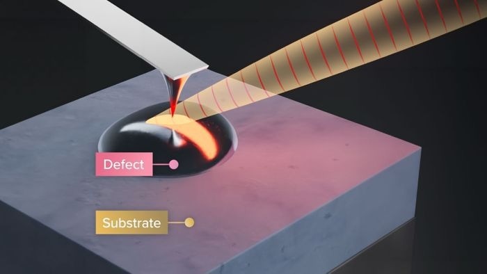
Image Credit: Park Systems
Applications
Ideal for Diverse Applications
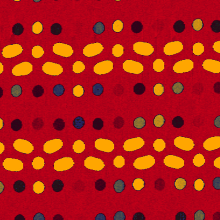
AFM Image Gallery. SRAM. Image Credit: Park Systems Corp
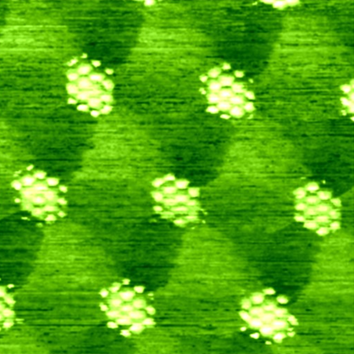
AFM Image Gallery. tBG/hBN. Image Credit: Park Systems Corp
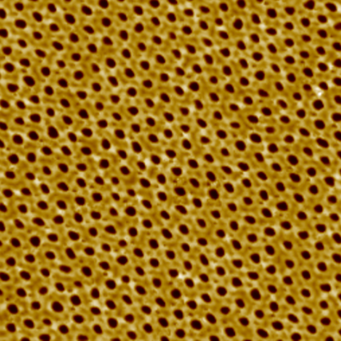
AFM Image Gallery. Organic SAM. Image Credit: Park Systems Corp
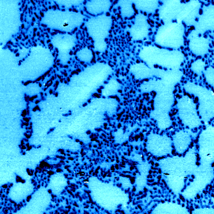
AFM Image Gallery. Aluminum alloy. Image Credit: Park Systems Corp
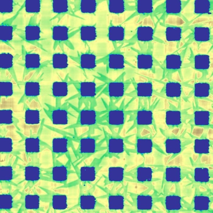
AFM Image Gallery. Cu pad. Image Credit: Park Systems Corp
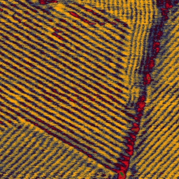
AFM Image Gallery. C36 alkanes. Image Credit: Park Systems Corp