LIG Nanowise and Nikon Metrology Europe jointly developed the LV-MOD, which is applicable in semiconductor imaging.
Source: LIG Nanowise Limited
| Relating to Part numbers |
| LVMOD-01-NIK |
| Physical Parameters |
| Dimension: |
160 x 140 x 232 mm |
| Weight: |
2.4 kg |
| Mounting diameter: |
52.5 mm |
| Mounting depth: |
17 mm |
| Fixing quantity: |
3 |
| Fixing type: |
M4 x 12 |
| Electrical Parameters |
| LV-MOD Voltage: |
15 Vdc |
| LV-MOD Power: |
6 W |
| LV-MOD Connection: |
2.5 (ID), 5.5 (OD) |
| LV-MOD Earthing: |
Ground 0 V |
| Mains Voltage: |
100-240 Vac |
| Mains Frequency: |
50/60 Hz |
| Mains Power: |
40 W |
| Mains Isolation: |
No. Earth connected to output 0 V. |
| USB |
USB Type B |
| Optical Parameters |
| Optical Power: |
1370 (typical) milliwatts (max) |
| Optical Peak Wavelength: |
440 nm |
| Optical Bandwidth: |
400-700 |
| Optical Risk Group: |
2 |
| SMAL Parfocality: |
No |
| SMAL AIR Parfocality: |
No |
| Environmental |
| Operating Temp Range: |
10-40 °C |
| Humidity: |
85 % RH non-condensing |
| Storage Temp range: |
0-40 °C |
Spatial resolution down to 60 nm demonstrated using semiconductor samples when coupled with the SMAL lens.
Semiconductor Imaging Application Example
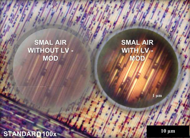
Image Credit: LIG Nanowise Limited