eWARP TKD is the latest iteration of Bruker's advanced eWARP detector family, with an advanced Wide ARea Pixelated (WARP) sensor design and engineered specifically for transmission EBSD (t-EBSD), also known as transmission Kikuchi diffraction (TKD).
The eWARP detector family has changed what is possible in EBSD with rapid acquisition speeds and exceptional spatial accuracy. Using the same core WARP design, eWARP TKD pushes the boundaries of t-EBSD, unlocking new opportunities for precise nanomaterial evaluation.
eWARP TKD is built for the characterization of nanoscale materials using an "on-axis" sample-detector geometry in scanning electron microscopy (SEM). eWARP TKD exceeds existing tranmission EBSD detectors across all critical parameters, delivering unparalleled sensitivity, acquisition speed, spatial resolution, and data integrity.
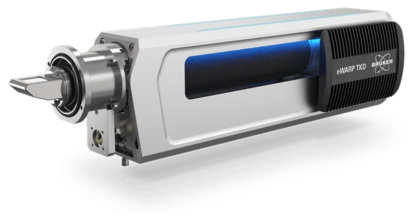
The eWARP TKD detector delivers unmatched throughput, spatial resolution, and data quality in nanomaterials characterization. Image Credit: Bruker Nano GmbH – Electron Microscope Analyzers
Take Nanomaterials Characterization to the Next Level with eWARP TKD
eWARP TKD redefines nanomaterial characterization in the SEM, providing key advantages for material researchers and engineers:
- Massive productivity gains: Delivers top-quality orientation and phase maps within one to five minutes at acquisition rates up to 5700 fps
- Integrated Dark Field (DF) and Bright Field (BF) imaging at lightning speed: Driven by patented eWARP on-chip binning technology
- Unmatched spatial resolution: Mapping precision below 2 nm spatial resolution
- No drift correction, minimal artifacts: Low beam-current demands and high-speed collection render drift compensation unnecessary and yield datasets virtually free of drift-related errors
- Time-resolved mapping during in situ experiments: Captures maps and images every few seconds to record dynamic microstructural shifts in thin specimens during in situ heating or mechanical testing
- Engineered for delicate samples: Exceptional signal processing permits low-dose, low-kV TKD mapping for beam-sensitive specimens
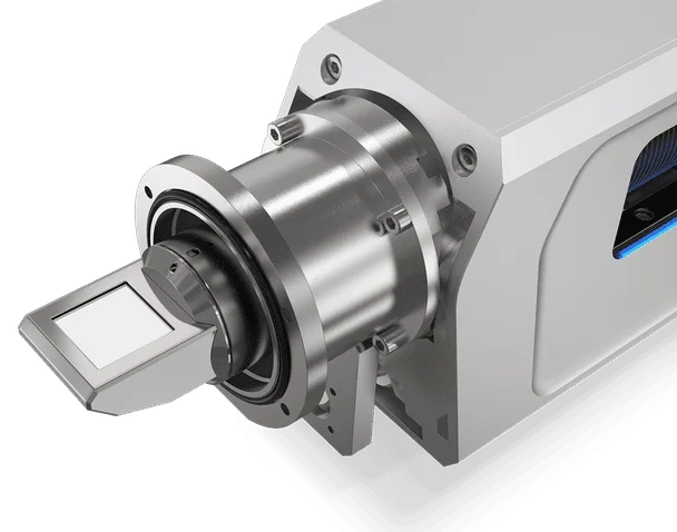
eWARP TKD uses a direct electron-detecting sensor with an active area of 26 x 26 mm2, oriented parallel to the specimen (On-Axis geometry) for TKD analysis. Image Credit: Bruker Nano GmbH – Electron Microscope Analyzers