XFlash® 7200 FIRE is an innovative energy-dispersive X-ray spectroscopy (EDS) detector designed for extremely rapid, high-resolution elemental analysis, even with demanding samples.
The detectors large active area consists of four separate SDD segments, each with its own pulse processing capability. This distinctive design enables the XFlash® 7200 FIRE to achieve top output count rates (OCR) of up to 2,400,000 cps, with an outstanding peak resolution across the entire EDS range and remarkable sensitivity to light elements.
XFlash® 7200 FIRE: Four-Segment Integrated Detector for Rapid EDS
The groundbreaking XFlash® 7200 FIRE transforms the possibilities of SEM EDS.
- Qualitative and quantitative EDS analysis at ultra-fast speeds
- Industry-leading count rates for elemental mapping down to the nanoscale
- Simultaneous 4x signal processing for extremely low dead times
- Analysis across the entire EDS spectrum up to 30 keV
- Low-energy X-ray sensitivity for light element detection
- Parallel analysis with our eWARP EBSD detector possible for rapid and comprehensive materials analysis
- Perform STEM-in-SEM EDS
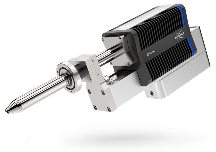
XFlash® 7200 FIRE is a trailblazing largest-in-class SD detector with a 2,400,000 cps OCR that redefines what is possible in SEM EDS. Image Credit: Bruker Nano GmbH – Electron Microscope Analyzers
Applications
Push the Limits of What Is Possible in EDS with XFlash® 7200 FIRE
The XFlash® 7200 FIRE detector is highly effective for challenging SEM EDS applications, including:
Semiconductor and Advanced Materials
With its exceptional spectral and spatial resolution the XFlash® 7200 FIRE detector excels in the analysis of advanced materials and semiconductors, which often have nanoscale features and contain elements with significant peak overlaps.
Battery Materials and Light-Element-Rich Samples
The XFlash® 7200 FIRE windowless design optimizes the detection of low-energy X-rays, allowing for the examination of battery materials, polymers, and other samples that contain light elements.
Nanostructured Samples
The capability to collect adequate EDS data quickly, even at low accelerating voltages, allows for the detailed characterization of samples that possess nanoscale characteristics.
Life Science and Beam-Sensitive Samples
By optimizing X-ray collection efficiency and processing capacity, the XFlash® 7200 FIRE enables the collection of statistically meaningful data at low electron doses for the examination of delicate samples such as biological materials.
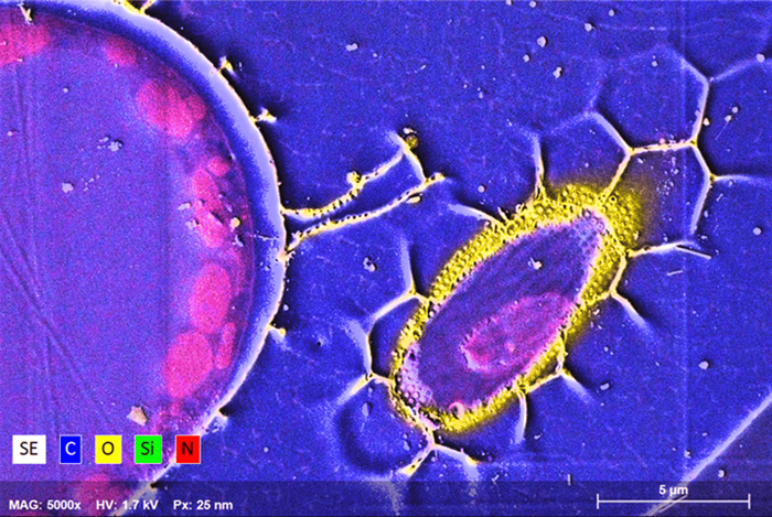
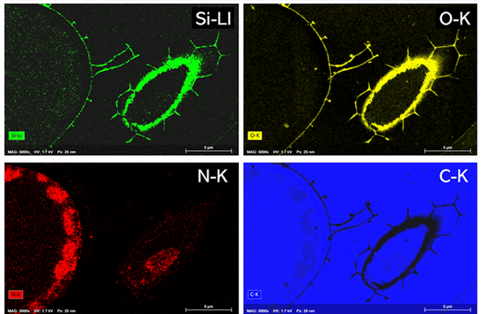
Ultra-low-kV SEM-EDS analysis of the diatom Stephanopyxis turris using the XFlash® 7200 FIRE. High collection efficiency and exceptional sensitivity to ultra-low-energy X-rays enabled elemental mapping at 1.7 kV and 1.6 nA probe current, giving an output count rate of 19,200 cps at only 1% dead time. At 1.7 kV, Si Kα is not excited, allowing chemical mapping of the nanostructured silica frustule exclusively through the Si L emission line (91 eV). The combination of low-kV excitation, high count statistics, and low electron dose enhances spatial resolution while minimizing specimen drift and beam-induced damage in this beam-sensitive biological sample. Image Credit: Bruker Nano GmbH – Electron Microscope Analyzers