SignatureSPM is the first microscope developed on a multimodal characterization platform. It integrates an automated atomic force microscope (AFM) with a Raman/Photoluminescence spectrometer to enable true colocalized measurements of physical and chemical properties.
The system provides reliable and comprehensive sample analysis by combining physical and chemical information in a single, real-time measurement. This approach reduces sample handling and shortens the time to insight while offering high-confidence data through the correlation of multiple measurement types.
Image Credit: HORIBA
Features
All AFM Modes Included as Standard
All AFM modes are included in the basic SignatureSPM package, including Kelvin Probe Microscopy, Piezo Response Force Microscopy, Magnetic Force Microscopy, Nanolithography, and Force-Curve Measurements.
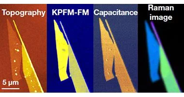
Image Credit: HORIBA
Wide Range Spectrometer Optimized for Raman and Photoluminescence
Designed for spectroscopic imaging, the SignatureSPM spectrometer features an achromatic design with 95% light reflectivity to minimize light loss. Its versatile configuration accommodates up to three gratings, enabling accurate and efficient Raman and photoluminescence (PL) measurements across a wide spectral range.
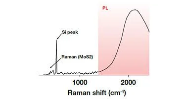
Image Credit: HORIBA
True Co-Localized Measurements with "Probe Away"
The "Probe away" software command moves the cantilever from the sample surface, allowing unobstructed acquisition of confocal Raman maps. The "Probe back" command automatically returns the AFM tip to its previous analysis position on the sample surface.
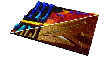
Image Credit: HORIBA
Direct Pathway to Cantilever Apex with High Optical Access
The optical pathways for AFM and spectroscopy are fully separated. This separation allows for a flexible selection of Raman/Photoluminescence (PL) laser wavelengths, simplifies system adjustments, and provides high magnification for precise visualization and positioning of the AFM tip.
Image Credit: HORIBA
AFM for Large Scans and Molecular Resolution
The SignatureSPM delivers exceptional AFM performance with stability and speed, thanks to its 100 × 100 × 15 micron-range scanner. It enables large scans with molecular resolution, emphasizing stability through fast response times, low noise, minimal drift, and metrological traceability.
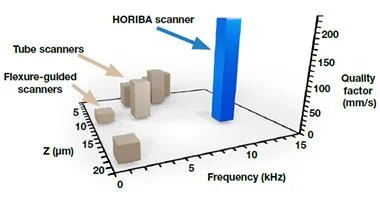
Image Credit: HORIBA
Quick and Repeatable Cantilever’s Adjustment
Seamless tip exchange is possible regardless of the operator, offering unmatched reproducibility. When replacing the cantilever, the same spot on the sample surface can be easily located and scanned with minimal effort, achieving repeatability within a few microns.
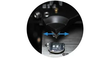
Image Credit: HORIBA
Automated AFM Registration System Adjustment
The fully automated alignment of the laser, cantilever, and photodiode is designed for seamless integration with optical spectroscopy, eliminating user intervention.
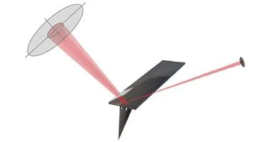
Image Credit: HORIBA
No Interference Between AFM Laser and Spectroscopic Measurements
The infrared AFM laser diode is non-interfering with the visible Raman/PL excitation lasers, preventing any parasitic influence on light-sensitive biological, semiconductor, and photovoltaic samples.
Image Credit: HORIBA
Applications
Colocalized AFM-Raman Analysis of 2D Materials Heterostructures
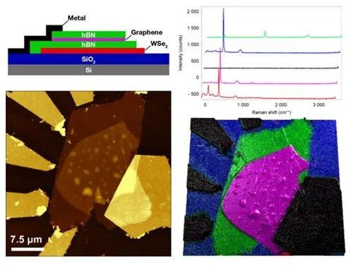
Image Credit: HORIBA
Van der Waals heterostructures, characterized by weak interlayer coupling and strong in-plane bonding, present exciting opportunities for designing novel materials with customized electronic, optical, and mechanical properties.
Colocalized AFM-Raman Analysis of Graphene
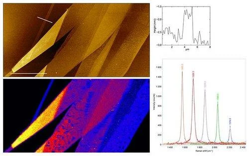
Image Credit: HORIBA
Graphene, a single layer of carbon atoms arranged in a two-dimensional honeycomb lattice, demonstrates exceptional electrical, thermal, and mechanical properties, making it a focal point of extensive research across various scientific disciplines.