The GD-Profiler 2™ from HORIBA offers rapid, simultaneous analysis of all elements of interest including nitrogen, oxygen, hydrogen and chlorine. It is an ideal tool for thin and thick film characterization and process studies.
Equipped with an RF source that can operate in pulsed mode for fragile samples, the range of applications of the GD-Profiler 2™ goes from corrosion studies to PVD coating process control, from thin-film PV development to LED Quality Control, and it is used in Universities as well as in Industrial Research laboratories.
Features
- The source can be pulsed with synchronized acquisition for improved outcomes on fragile samples. Using an RF source enables the analysis of conventional and non-conventional layers and materials.
- RF-Only generator is Class E standard and is optimized for stability and crater shape, thereby enabling real surface analysis.
- Simultaneous optic offers complete spectral coverage varying from 110 to 800 nm, such as deep UV access to examine H, C, O, N, and Cl.
- Patented HDD detection offers sensitivity and speed in detection without making any compromises.
- HORIBA original, ion-etched holographic gratings guarantee the greatest light throughput and resolution for utmost light sensitivity and efficiency.
- An easily accessible sample compartment enables a great deal of room for sample loading.
- On-line measurement of erosion rate and crater depth with patented built-in Interferometer. DIP.
- CenterLite laser pointer (patent pending) for accurate sample loading.
- String QUANTUM™ software available with Tabler report writing tool
The monochromator option is only available from HORIBA and is the perfect tool to increase instrument flexibility while adding "n+1" capability.
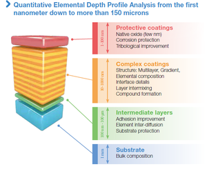
Image Credit: HORIBA
Specifications
This is a combination of a powerful Glow Discharge source with Ultra-Fast High Resolution simultaneous optics for fast Elemental Depth Profile Analysis of conductive, non-conductive and hybrid materials.
It is ideal for thin and thick films - from nanometers to hundreds of microns along with nanometer depth resolution.
- Typical domains of applications such as PV, LED manufacturing, metallurgy, corrosion studies, organic, and micro-electronics, materials research and development, deposition processes optimization, CVD, PVD, plasma coatings, Li batteries, and automotive, etc.
- Measurement of all elements of interest (such as H, O, D, Li, C, Na, N, etc.) with patented High Dynamic Detectors.
- No UHV required.
- Pulsed RF Source for operation in RF and pulsed RF modes with auto-matching
- Optional monochromator with Image mode and high Dynamic detection for full spectrum record and total flexibility.
- Differential double pumping of the source for patented SEM sample preparation
- Patented UFS available for Ultra-Fast Sputtering of polymeric and organic materials
- Plasma Cleaning function built in
- Patented DIP–built in interferometer for direct on-line depth measurement
- Various anode diameters and accessories for odd shape samples
- Windows 10 Software: Several copies are offered for remote installations