With a minimum probe diameter of 3 nm SEI and 8 nm for Auger analysis, the JAMP-9510F Field Emission Auger Microprobe provides the highest spatial resolution of any Auger microprobe.
The JAMP-9510F achieves extremely small spot sizes with beam currents up to 200 nA by using a patented “in-lens” Schottky field emission gun in conjunction with a low-aberration condenser lens, which superimposes an electrostatic field and a magnetic field.
Key Features
Spectrum Imaging
A recently developed hyperspectral mapping technique allows the creation of elemental maps from full spectral data cubes. In traditional Auger mapping, users must specify elements beforehand, which could lead to incomplete data sets.
Auger maps can now be made for any element using a hyperspectral method akin to EDS. To generate the hyperspectral data set, either choose the measured energy range and resolution or employ wide-spectrum acquisition. Both elemental analysis and reflection electron energy loss (REELS) analysis can benefit from the use of hyperspectral imaging.
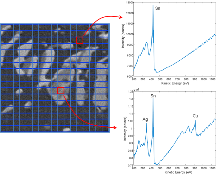
Each pixel contains spectrum. Image Credit: JEOL USA, Inc.
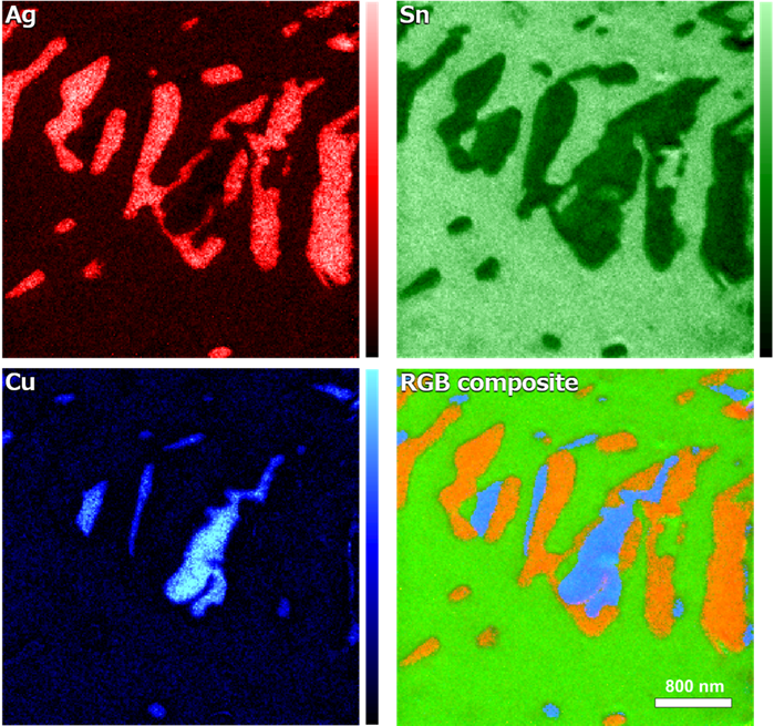
Elemental distributions extracted from a spectrum image data cube. Image Credit: JEOL USA, Inc.
Standard Spectra Database and Peak Deconvolution Software
Complex chemical state analysis is made possible with a single click, thanks to standard spectra and integrated peak deconvolution software. The company has over 500 spectra for 140 materials in the standard spectra database.
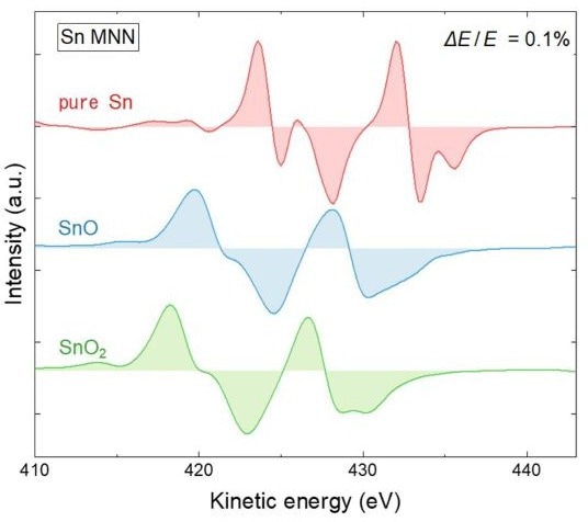
Standard spectra of pure Sn, SnO and SnO2. Image Credit: JEOL USA, Inc.
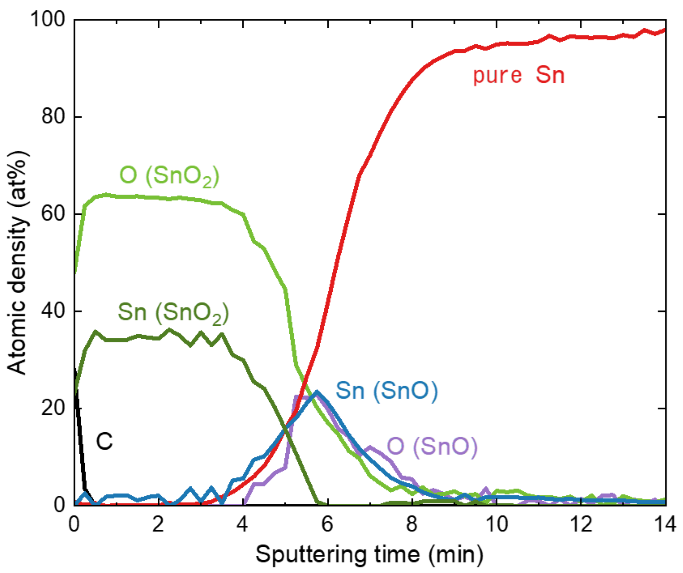
Chemical-state resolved depth profile of the solder surface. Image Credit: JEOL USA, Inc.
Specifications
Source: JEOL USA, Inc.
| |
|
| Electron illumination system |
| SEI resolution |
3 nm(at 25 kV, 10 pA) |
| Probe diameter for Auger analysis |
8 nm(at 25 kV, 1 nA) |
| Electron gun |
Schottky field emission gun |
| Accelerating voltage |
0.5 to 30 kV |
| Probe current |
10-11 to 2×10⁻⁷ A |
| Magnification |
x 25 to 500,000 |
| Auger analysis system |
| Analyzer |
Electrostatic hemispherical analyzer (HSA) |
| Energy resolution(ΔE/E) |
0.05 to 0.6% |
| Sensitivity |
840,000 cps/7 ch or more (at 10 kV 10 nA Cu-LMN, 0.6% resolution, 60 tilt) |
Expandability
There are extra ports available to support a range of analyses, as well as the following attachments:
- Specimen Cooling and Fracturing Device
- Specimen Parking Unit
- Energy Dispersive X-ray Spectrometer (EDS)
- Backscattered Electron Detector
- Transfer Vessel
Application
Semiconductor Devices
When compared to other X-ray emission spectroscopy methods like SEM-EDS and EPMA, AES provides exceptional spatial resolution for describing features that are smaller than 100 nm. Chemical state analysis, including chemical state mapping, is also made possible by this technique's high spectral resolution.
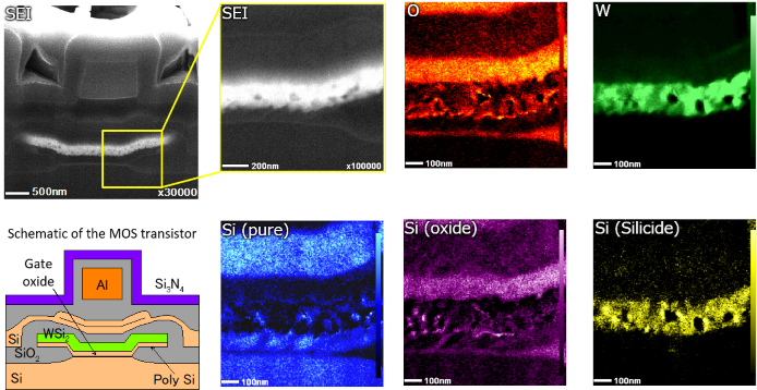
Elemental distributions and chemical state mapping of silicon of a cross-section of a semiconductor device, acquired by spectrum imaging. Image Credit: JEOL USA, Inc.
Lithium-Ion Battery (LIB) Materials
AES has a high sensitivity for lithium detection and is frequently used to analyze the materials of lithium-ion batteries. As electrons at nearby atoms participate in the auger process, AES has a high sensitivity for detecting lithium peaks from lithium oxides and carbonate. Spectrum imaging makes lithium mapping simple to accomplish.
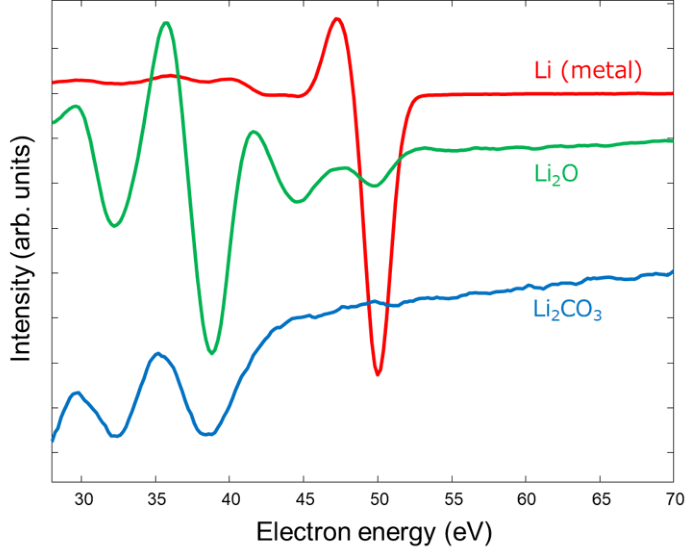
Standard spectra of Li KVV in the differential form. Image Credit: JEOL USA, Inc.
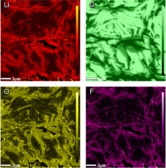
Cross-section elemental mapping for a LIB anode material. Image Credit: JEOL USA, Inc.
REELS Analysis
REELS, or reflection electron energy loss spectroscopy, is another significant use for Auger microprobes. In addition to analyzing carbon materials, REELS is used to assess the bandgap size of insulators and wide-bandgap semiconductors.
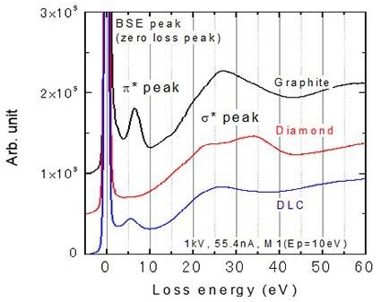
Loss spectra of carbon materials. Image Credit: JEOL USA, Inc.
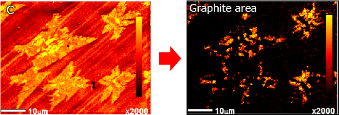
Carbon distribution obtained by AES analysis (left) and graphite distribution by REELS analysis (right) for a graphene sample on a copper plate. Image Credit: JEOL USA, Inc.