Here are some of the features of JBX-A9: Electron Beam Lithography System.
- In-line extendibility to other process tools, such as coaters and developers
- Minimal power consumption
- Enhanced ease of use for users of all skill levels
- A direct writing system with high precision and high throughput
- Designed with JEOL’s famous Electron Optics for maximum stability
- Loadable wafer up to 300 mm
- FOUP system is optionally available
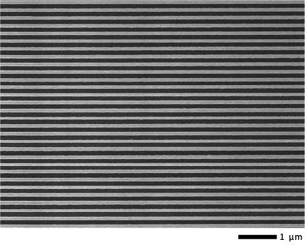
DFB Laser / Nanoimprint. Image Credit: JEOL USA, Inc.
Metalens. Image Credit: JEOL USA, Inc.
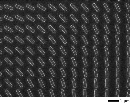
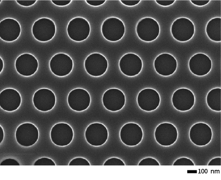
Lens Arrays. Image Credit: JEOL USA, Inc.
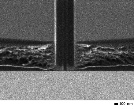
T-Gate. Image Credit: JEOL USA, Inc.
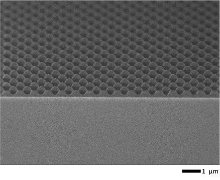
Photonic Crystal. Image Credit: JEOL USA, Inc.
Source: JEOL USA, Inc.
| Basic Configuration |
| Basic Unit |
| 10 Cassettes Auto Loading System |
| Control Program with CPU System |
| Additional License for Data Preparation Program |
| Remote Control OL Aperture |
| Options |
| In-situ Optical Microscope |
| FOUP Wafer Auto Loading System |
| Open Cassette 200 mm Wafer Auto Loading System |
| 48 kV High Voltage Program |
| Custom Cassettes |
| SECS/GEM |
| Air Conditioner |
| EMI cancellation system |
JBX-A9 Series Specifications. Source: JEOL USA, Inc.
| Item |
Specification |
| Accelerating Voltage |
100 kV |
| Maximum Field Size |
1000 μm |
| Minimum Increment |
0.25 nm |
| Stitching Accuracy |
±9 nm |
| Overlay Accuracy |
±9 nm |
| Minimum Line width |
≦8 nm |
| Beam Current |
50 pA to 400 nA |
| Maximum Scanning Speed |
200 MHz |
| Stage Positioning Resolution |
0.15 nm |
| Automatic Aberration Corrections |
Dynamic Focus
Dynamic stigmatism
Deflection Distortion Correction |
| Maximum Sample Size |
300 Wafer
9-inch Mask |
| Power Consumption |
5 kVA |
| Footprint |
7.4 m × 5.3 m × 2.7 m (H) |