The LabRAM Odyssey Semiconductor microscope is excellent for photoluminescence and Raman imaging of wafers up to 300 mm in diameter. The HORIBA best-seller true confocal microscope comes with an automated 300 mm sample stage and an objective turret to meet the needs of wafer uniformity assessment and flaw detection.
Features
LabRAM Odyssey Semiconductor consists of hardware and software designed for semiconductor analysis.
- Wafer mapping with automated turret and sample stage
- The automated 300 mm × 300 mm XY sample stage accommodates wafers up to 300 mm (12”) diameter for Raman and Photoluminescence mapping of complete wafers and tiny ROIs. The stage's movement speed, together with its stability, ensures quick and consistent measurements of ROIs dispersed across the wafer surface.
- Uniformity measurement with wafer tilt correction
- The "Tilt at Midway" autofocus mode compensates for any wafer bow and tilt, resulting in accurate entire wafer uniformity data, even from thin layers. This function is quick because it finds the best focus height at only five points before mapping: the center and four points halfway between the center and the corners.
- From full wafer to high-resolution defect mapping with DuoScan™
- DuoScan™ confocal imaging technology combines variable-size laser macro-spot scanning (with ultra-fast rastering mirrors) and high accuracy sub-micron step scanning. Macro-spot scanning is appropriate for whole wafer mapping, but sub-micron step scanning is ideal for defect analysis
- PL and Raman metrology in one tool
- The availability of numerous excitation lasers, together with the system's wide spectral range, from deep UV to near IR, enables simultaneous detection of photoluminescence and Raman signals in the same spectrum. Combining PL and Raman in one tool dramatically accelerates wafer characterization
- Methods: Easy recipe building for highly efficient characterization
- Methods will allow the user to fully automate their entire Raman/PL characterization procedure (collection, data processing, display, and analysis), resulting in a high throughput that metrology technicians can manage
- The “methods” creation procedure is straightforward and intuitive: the process or metrology engineer can optimize each operation and then incorporate it into the recipe/method with a single click. Individual processes can be readily rearranged, added, or omitted
- This customization feature is also supported by “templates,” which allow users to save and recall a set of hardware configurations and software preferences
- ParticleFinder PF3: Automated particle characterization
- PF3 quickly locates and chemically identifies contaminants on a full wafer
- PF3 automatically detects and maps contaminated particles. PF3 also recognizes and classifies all discovered contaminants based on their chemical properties (organic, silicon, etc.)
- Statistics on morphological parameters (area, perimeter, diameter, circularity, brightness, volume estimation, etc.) are also provided
Specifications
Source: HORIBA
| . |
. |
| Dimensions |
W × H × D (mm): 1400 × 620 × 1410 |
| Optical microscope |
Open space microscope with white light reflection illumination, camera, 5×, 10×, 100× objectives as standard. Optional motorized objective turret. |
| Spectral range |
Standard 200 nm - 2200 nm from sample to detector (achromatic, no change of optics required). |
| Imaging spectrometer |
- Focal length: 800 mm.
- Spectral resolution FWHM at 532 nm excitation wavelength ≤ 0.6 cm-1 with 1800 gr/mm and ≤ 0.3 cm-1 with 3000 gr/mm.
- Spectral stability RMS: < 0.02 cm-1 RMS Measured on Si 520 cm-1 line.
- Equipped with Open Electrode CCD (standard), optional EMCCD, optional InGaAs arrays detector (max. 3 detectors).
|
| Spatial resolution |
XY lateral resolution < 0.5 µm; Z axial resolution < 1.5 µm. |
| 300 mm × 300 mm motorized stage |
XY high precision encoded motorized stage (X = 300 mm, Y = 300mm) with repeatability ≤1 µm; accuracy = 1 µm; resolution (encoder) = 50 nm; minimum motor step size = 10 nm.
Z specifications: resolution (minimum step size) = 0.01 µm.
Holders for 4" (100 mm), 6" (150 mm), 8" (200 mm) and 12" (300 mm) size wafers available. Vacuum compatible wafer holders. |
| Lasers |
User selectable: 266 nm, 325 nm, 355 nm, 405 nm, 458 nm, 473 nm, 532 nm, 633 nm, 660 nm, 785 nm, & 1064 nm. Up to 6 motorized. |
| DuoScan™ |
DuoScan™ technology for fast Laser scanning and Macrospot imaging (typical macrospot dimensions 30 µm × 30 µm with 50× objective). |
Applications
2D Materials
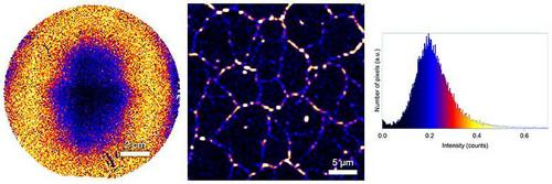
Image Credit: HORIBA
Two-dimensional graphene and transition metal dichalcogenides materials are poised to become the foundation of future electronic gadgets. Controlling layer counts and crystallinity on a wafer scale remains the primary difficulty.
Group IV Semiconductors
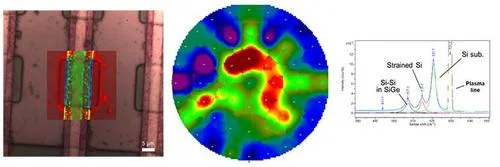
Image Credit: HORIBA
The historically established group IV materials remain essential to integrated circuits despite more sophisticated topologies (three-dimensional: FinFET, Nanosheet FET, Gate-all-around FET).
Compound Semiconductors
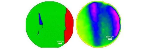
Image Credit: HORIBA
Compound semiconductors, such as III-V, III-N materials, and SiC, are increasingly used due to their superior material properties over silicon semiconductors and their role in improving device energy efficiency.